
![]()
![]() Narrow down by specifying conditions
Narrow down by specifying conditions
現在1889件がヒットしています。check

Temperature characteristics and performance during switching of Qorvo SiC FET
Qorvo 's SiC FET product lineup is built on a core technology that combines high-voltage normally-on SiC JFETs and low-voltage normally-off Si MOSFETs in a cascode configuration. Figure 1 shows a simple cross-sectional structure of a general SiC MOSFET and Qorvo 's cascode-connected SiC FET.
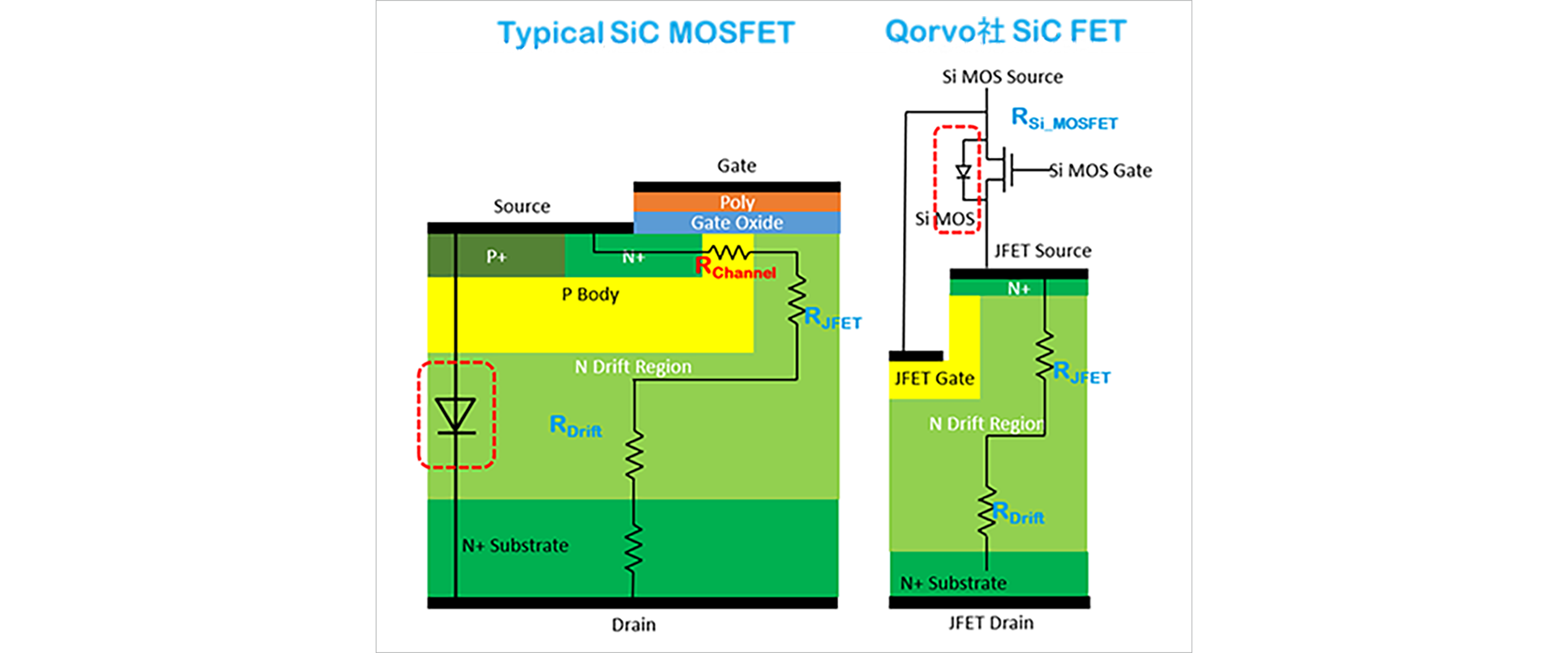
Figure 1: Schematic cross-sectional diagram of a typical SiCMOSFET and Qorvo SiC FET
The problem with switching loss in power circuits is the "reverse recovery loss" that occurs every time the body diode conducts. Due to conduction, a charge Qrr is accumulated in the body diode. Then, when reverse biased, a recovery current flows to discharge the accumulated charge Qrr, causing loss. This body diode action results in higher peak power dissipation and lower efficiency as the switching frequency increases.
For Si MOSFETs, switching losses can be significant. For example, in some circuits, such as the common totem-pole PFC that operates in continuous conduction mode (CCM), Si MOSFETs are not practically used due to their high losses. The stored charge Qrr also depends on the withstand voltage of the device. Figure 2 compares Qorvo 's SiC FET and Si superjunction MOSFET with similar ratings. Comparing the reverse recovery waveforms of the body diodes, you can see that Qorvo 's SiC FET has a shorter reverse recovery time.
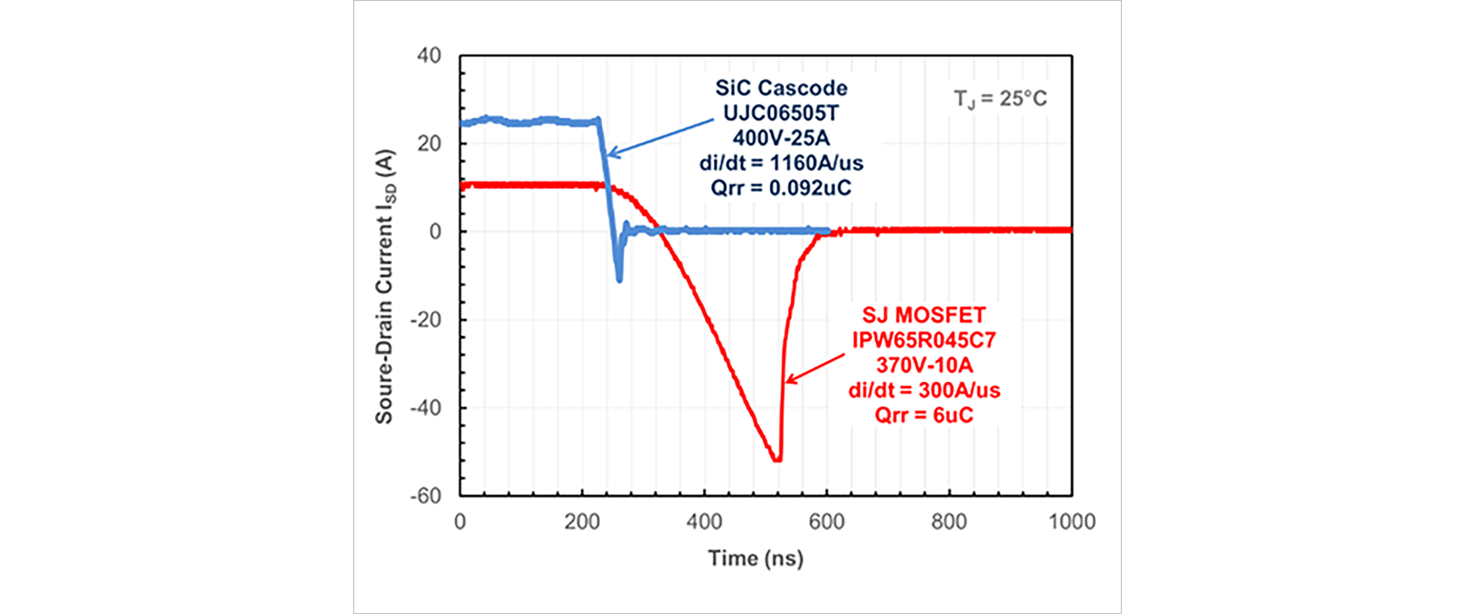
Figure 2: Comparison of current waveforms during reverse recovery between SJ MOSFET and Qorvo's SiC FET
Qrovo SiC FET Features ①: Short reverse recovery time
The storage charge Qrr of SiC MOSFET is 10 times better (less than 1/10) than that of Si MOSFET. But Qorvo 's SiC FETs are even better than that. This is because the output capacitance of the SiC JFET, which has a cascode configuration, is small, and the charge accumulated in the body diode of the low-voltage Si MOSFET, which is responsible for ON/OFF, is small.
Figure 3 shows waveforms comparing the reverse recovery times of a SiC MOSFET and Qorvo 's SiC FET. The accumulated charge Qrr of SIC MOSFET is 220nC. The body diode of a SiC MOSFET has a high forward voltage drop, VF, so if VF is too high, connect a SiC Schottky barrier diode in parallel. Qrr at that time is 275nC. On the other hand, the Qrr of the body diode of Qorvo 's SiC FET is as low as 105nC, which contributes to reducing switching loss.
Qrovo SiC FET feature ②: Reverse recovery loss does not increase even if the temperature rises
The data in Figure 3 was measured at 150 °C, 800V, and 11A. The Qrr of the body diode of Qorvo 's SiC FET does not change much even when the temperature changes, and Qrr only increases by 10% when the temperature changes from 25 °C to 150 °C. The reason is that most of the Qrr of Qorvo 's SiC FET is generated from the output capacitance Coss of the SiC JFET. Since it is a capacitive charge, it does not increase with temperature. Some Qrr comes from the body diode of the Si MOSFET and increases with temperature, but overall it only increases by 10%.
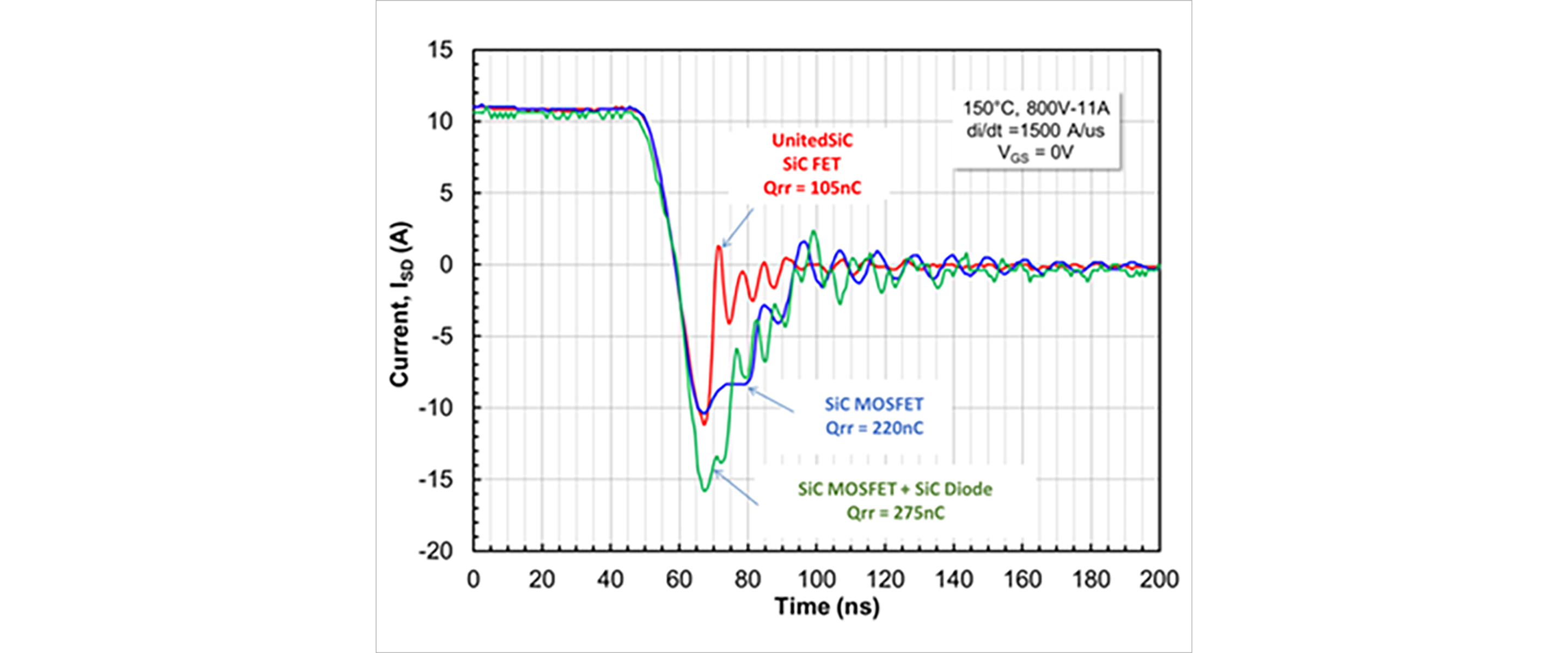
Figure 3: Comparison of current waveforms during reverse recovery between SiC MOSFET and Qorvo's SiC FET
Qrovo SiC FET feature ③: Almost no mirror capacitance
The SiC JFET that makes up Qrovo 's SiC FET has almost no drain-source capacitance Cds. Strictly speaking, since the electrodes are opposing each other, the value is not completely zero, but it is extremely close to zero. Considering the gate-drain capacitance Cgd as Qrovo 's SiC FET in Figure 4, the drain-source capacitance Cds_sic of the SiC JFET and the gate-drain capacitance Cds_si of the Si MOSFET are connected in series, so the combination The resulting Cds will be a very small value.
This means that the feedback capacitance Crss (=Cgd) is small, and when used as a synchronous FET in a synchronous rectification method, there is very little risk of erroneous turning on due to a steep rise in the switch node.
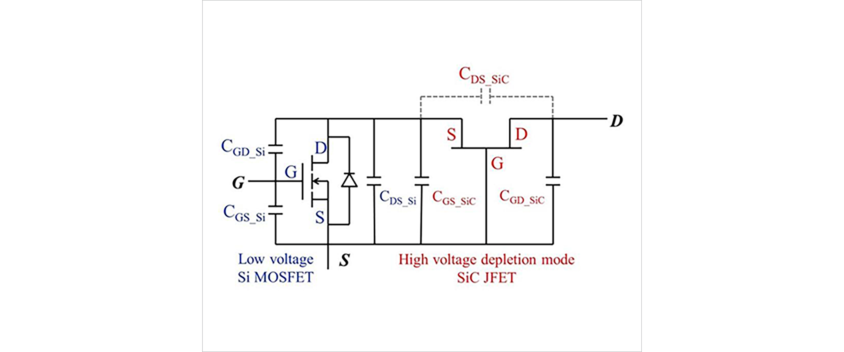
Figure 4: Parasitic capacitance of Qorvo's SiC FET
FETs have parasitic capacitance as shown in Figure 5. When the drain voltage increases rapidly, the gate potential changes depending on the ratio of Cgd and Cgs capacitance. The effect is particularly large when the drain voltage is high. When the drain voltage changes from zero to 600V, the gate potential changes by 6V if the Cgs/Cds ratio is 1/100. Care must be taken when the gate driver has a high output impedance.
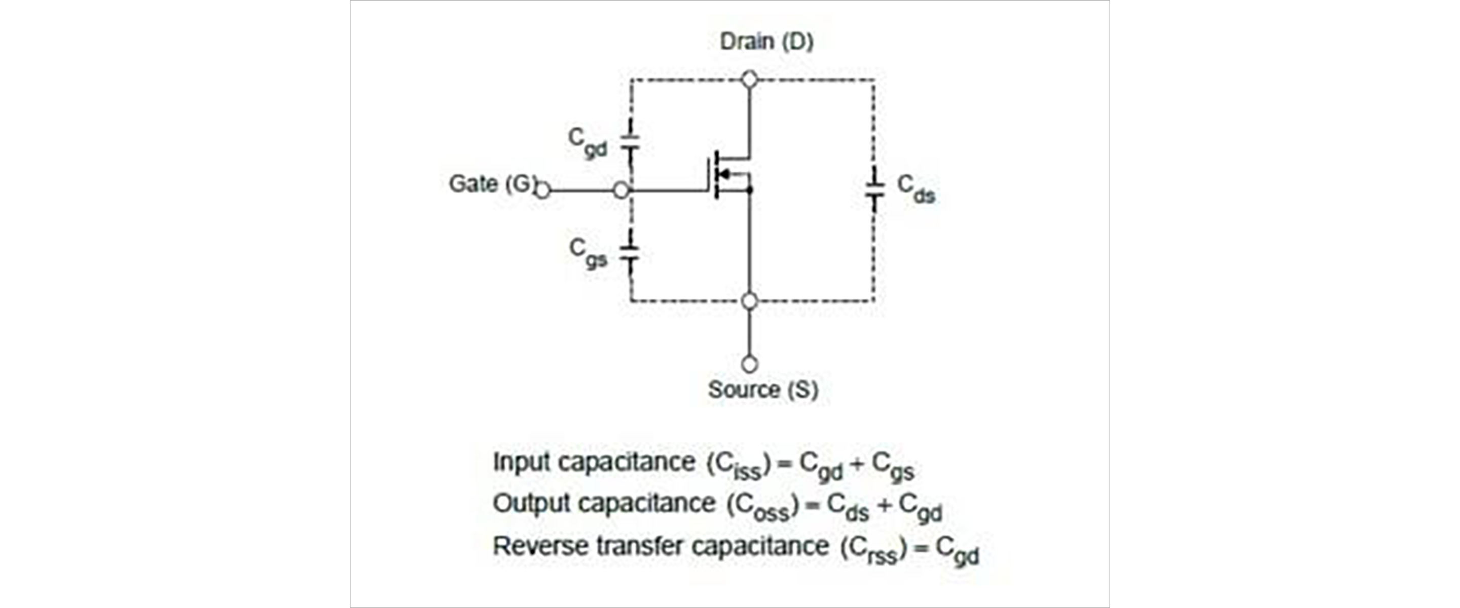
Figure 5: Parasitic capacitance of Qorvo's SiC FET
Table 1 is an example of parasitic capacitance extracted from the actual data sheet of Qorvo 's SiC FET (UJ4SC075006K4S). In this example, the Cgs/Cds ratio is 4/(8374-4)=1/2092, and the gate potential fluctuates by less than 0.3V for a change in drain voltage of 600V, so the possibility of false ON is very low. Become.
|
Parameter |
Symbol |
Test Conditions |
Value |
Units |
| Input capacitance |
Ciss |
VDS=400V、VGS=0V f=100kHz |
8374 |
pF |
| Output capacitance |
Coss |
362 |
||
| Reverse Transfer capacitance |
Crss |
4 |
Table 1: Parasitic capacitance of Qorvo SiC FET UJ4SC075006K4S
Inquiry
If you have any questions regarding this article, please contact us below.
To manufacturer information top page
If you want to return to Qorvo manufacturer information top page, please click below.
