
![]()
![]() Narrow down by specifying conditions
Narrow down by specifying conditions
現在1887件がヒットしています。check

Performance is a subjective term. Performance can be measured as much as you like. However, in the world of power conversion, it comes down to two key interdependent values: efficiency and cost. It is a well-known fact that silicon, the material of semiconductor switches, has reached its limits in terms of both conduction loss and switching loss, and wide bandgap technologies such as silicon carbide and GaN are being considered to improve performance. There are many.
The excellent breakdown properties of these materials allow thinner, more highly doped blocking layers to achieve low on-resistance, and the smaller die size reduces device capacitance and lowers switching losses. can. SiC MOSFETs and GaN HEMT transistors require tightly controlled gate drive conditions for optimum performance, and although they have lower losses than silicon, they are actually a disadvantage as wide bandgap devices. There is also
It also suffers from various differences with silicon switches, such as the gate threshold variation and hysteresis of SiC MOSFETs, and the lack of avalanche rating of GaN.
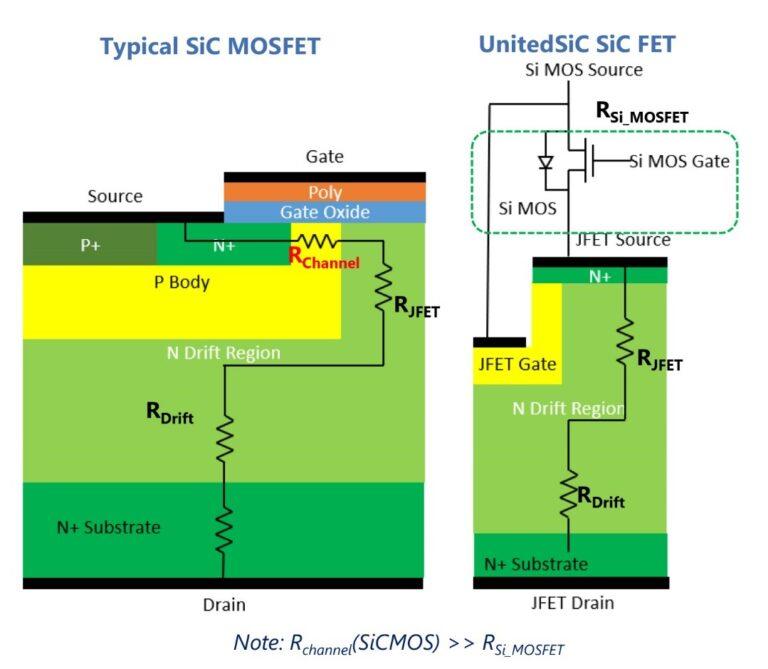
SiC FET approaching the ideal switch
Getting closer to the ideal, practical switch isn't necessarily a giant leap. simple vertical trenchSiC JFETsand silicon MOSFETs provide even lower normalized overall losses, easy, non-critical gate drive, and robust parts with high avalanche and short-circuit ratings. This device is a SiC FET cascode, Figure 1(Right), compared with the SiC MOSFET on the left. In the SiC FET, the channel resistance Rchannel of the SiC MOSFET is replaced with the resistance of a low-voltage Si MOSFET, and the electron mobility in the inversion layer is remarkably improved, resulting in low loss.
Also, SiC FETs have a smaller comparative die area, especially since they employ packages with Si MOSFETs stacked on top.
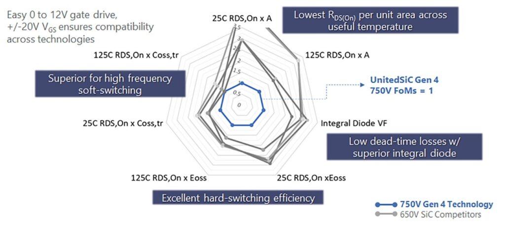
To compare actual performance,"Figure of Merit (FoM)"is best used. This FoM combines the contributions of conduction and switching losses for various applications at a given die size, which has important implications for yield per wafer and thus cost. Figure 2 are available 650V SiC MOSFETs and Qorvo's 750V,4th generation SiC FETsare compared. RDS(ON) xA (on-resistance per unit area) is the key FoM, the smaller the value, the smaller the die area for a given loss performance and the higher the yield per wafer.
Another FoM RDS(ON)xEOSS (On-resistance times the output switching energy) characterizes the trade-off between conduction and switching losses and is important in hard-switching applications. FoMRDS(ON)xCOSS (tr)shows the relative efficiency performance in high-frequency soft-switched circuits from the relationship between on-resistance and time-dependent output capacitance. Also, an important comparison is the forward voltage drop of the internal diode.
SiC FETsIn , VF is the sum of the body diode drop of the Si MOSFET and the resistance drop of the JFET in the 3rd quadrant, which sum is around 1-1.5V. For SiC MOSFETs, this number can be 4V or more, and applications that rectify current with internal diodes will experience significant conduction losses during switching dead time. The on-resistance-related FoM in the figure is shown at 25°C and 125°C, demonstrating the excellent performance of SiC FETs in actual usage environments.
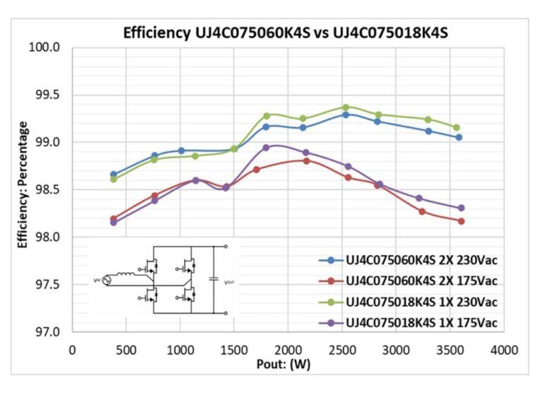
3.6kW SiC FET Totem Pole PFC Stage Demonstrator Achieves Peak Efficiency of 99.3%
Perhaps the best demonstration of SiC FET performance is a typical application, the totem-pole PFC stage. Although this circuit has long been known to be a potentially high efficiency solution for combining AC line rectification and power factor correction, it suffers from hard switching at high power and unacceptable switching losses in silicon MOSFET technology. loss will occur.
SiC FETs solve this problem, with a 3.6kW demo by Qorvo showing a peak efficiency of 99.3% at 230V AC, helping to more easily achieve efficiency ratings for 80+ Titanium systems. (Fig. 3). The two 18mΩ SiC FETs in the "fast" leg of the circuit consume only 8W each, while the "slow" leg uses silicon MOSFETs as synchronous AC line rectifiers. Replacing these with silicon diodes can provide a lower cost solution while still achieving efficiencies of over 99%. Figure 3 also shows the results of placing 60mΩ SiC FETs in parallel and one 18mΩ SiC FET in each switch on the “fast” leg.
SiC FET selection made easy with simulation tools
Qorvo's 'FET-Jet Calculator' makes it easy to select the best SiC FET components for optimum performance. This free-to-use, web-based tool allows users to select the desired design from a range of rectifiers, inverters, or isolated and non-isolated DC/DC topologies. Then enter your operating specifications and select your device from Qorvo's selection of SiC FETs and diodes. The tool instantly calculates efficiency, component losses (percentage of conduction and switching contributions), junction temperature rise, and more. Device parallelization effects are supported, and practical heatsink performance can also be specified.
Simulation and practical results show that SiC FETs can significantly improve the performance of power converters. Considering system effects, SiC FETs are also superior in this regard. Increased efficiency and faster switching reduce the size and cost of heatsinks and magnetics, leading to overall system balance and lower cost of ownership.
Inquiry
If you have any questions regarding this article, please contact us below.
Qorvo manufacturer information top page
If you want to return to Qorvo manufacturer information top page, please click below.
