
![]()
![]() Narrow down by specifying conditions
Narrow down by specifying conditions
現在1887件がヒットしています。check

Ask a power converter designer what they want from a solid-state switch and they might answer something like this: "low on-resistance, high off-resistance, and the fastest possible transition between two states". Of course, in simple terms, this translates into lower power consumption. SiC FETs are close to this ideal, with an on-resistance of 6mΩ or less in the 750V class, an edge rate in the nanosecond range, and efficiencies of 99.5% or more can be expected for converters and inverters of several kW class.
Designers may want to include a few niggles such as easy gate drive, high voltage rating, efficient 3rd quadrant operation, high avalanche energy and short circuit rating, low thermal resistance, and low system cost. Fortunately, SiC FETs cover these factors as well, with best-in-class figures of merit.
But if you run SiC FETs on a breadboard at their maximum slew rate, they quickly start to smoke. "Even though the supply voltage was well below the maximum and the load was light." Now, how much wiring and connection inductance was there? A staggering current edge rate of 3000A/µs with just 100nH of inductance causes a 300V voltage spike from the familiar equation V = -L*di/dt to stress the switch. It induced microsecond high-frequency ringing for a short period of time before the SiC FET broke down.
We now know that unless the connection inductance is zero, or the switch voltage rating is greatly overspecified and EMI filters are extensively used, the edge rate should be controlled to dampen the ringing. The traditional method of suppressing voltage spikes is to add a gate resistor RG(OFF) in series, but this is problematic and introduces a delay in the waveform, one of the greatest advantages of wide bandgap switches. duty cycle and high frequency operation are limited. Also, gate resistors only add significantly to switch losses and have little ringing damping effect.
A better solution is a simple RC snubber. You may shy away from the large, hot resistor and capacitor networks typically required for IGBTs, but not for SiC FETs. Snubbers are primarily used to dampen the resonance between the connection inductance and the device capacitance, which SiC FETs have very little capacitance. In other words, a capacitance of about 200pF (twice or three times Coss(er)) and a series resistance of several ohms will generally provide sufficient damping effect. Some power is dissipated in the snubber resistor, but this network serves to reduce the overlap of switch-off voltage and current in both hard-switched and soft-switched applications, so this transition loss is actually will be less.
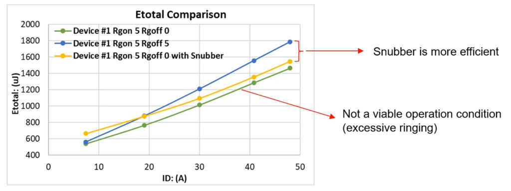
A snubber generates a slight loss at turn-on, so total loss E(ON) + E(OFF) must be taken into account in order to grasp the overall picture. The figure shows E(TOTAL) for 40mΩ. The blue line is the case without snubbers and both RG(ON) and RG(OFF) are 5Ω. The yellow line is for RG(ON) of 5Ω and RG(OFF) of 0Ω with a 200pF/10Ω snubber. Using a snubber at 40A has an obvious net benefit of about 10.9W loss reduction while operating at 40kHz. At light loads the situation is reversed, but losses are low at this level.
Estimated energy absorbed by the snubber resistor in a typical application is about 120 µJ per cycle, equivalent to about 5 W at 40 kHz. However, evaluation has shown that most of this energy is dissipated as the channel of the SiC FET passes through the linear region during turn-on, rather than in the snubber resistance. As a result, a 1W resistor is usually sufficient for a snubber, and at this power level surface-mount type resistors can easily be used. Also, the capacitor can be made smaller.
Designers can easily and cheaply adjust by adding a snubber circuit to reduce overshoot and ringing without compromising other benefits.
Inquiry
If you have any questions regarding this article, please contact us below.
Qorvo manufacturer information top page
If you want to return to Qorvo manufacturer information top page, please click below.
