
![]()
![]() Narrow down by specifying conditions
Narrow down by specifying conditions
現在1888件がヒットしています。check

It's funny how things can get better or worse depending on how you look at them. The perfect switch has existed since the dawn of electricity. At least eighteenth-century experimenters like Volta thought so and used brass, wood, and porcelain to build electrical isolators. There is almost no resistance in the closed state, "no leaks in the open state", "depending on the size of the capacitor, it can withstand any amount of voltage", this solved the problem.
A semiconductor that takes a step back from the ideal
The first electronic switches, vacuum tubes, were large, lossy, and fragile. Early transistors were a step back, except that they had high resistance and low breakdown voltage, and could be flipped much faster than their mechanical counterparts. Although the transistor had a small profile, it could only carry a small amount of current. Seventy-five years after Shockley et al.'s discovery, engineers have been striving to return to Volta's ideal solution, but at the same time they must switch faster at MHz speeds, while remaining small and current rated. There was also pressure to raise
The application that has driven the transistor to higher power is, of course, the switched mode power supply (SMPS), which enables highly efficient DC/DC power conversion without the need for a motor generator set. The SMPS idea was patented in 1959, and in 1970 the bipolar junction transistor (BJT) was first used in the Tektronix 7000 Series oscilloscopes. BJTs were successful in this application, but they were difficult to drive efficiently at high power, and switching losses were unacceptable above tens of kHz.
Fast, easy-to-drive MOSFETs were patented in 1960, but early versions had high on-resistance and high power loss at high currents due to the I2R "squared" term. I was. The breakthrough, however, was the invention of the IGBT, which had the ideal combination of the gate-drive ease of a MOSFET and the on-characteristics of a BJT, making it a practical solution for ultra-high-power converters to this day. I'm here. But "practical" is not "ideal". To avoid unacceptable dynamic losses in high-power applications, the switching frequency of the IGBT must be kept below about 10KHz, requiring the use of large, heavy, and expensive magnetic components. On the other hand, MOSFETs capable of switching up to about 500 kHz have evolved into the latest "super junction" type, and are now mainstream in the low and medium power areas of DC/DC and AC/DC.
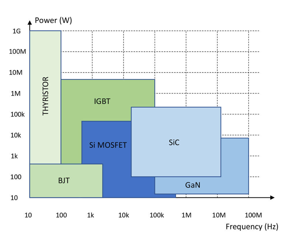
Wide bandgap semiconductors such as silicon carbide and gallium nitride are being investigated to close the application gap between IGBTs and silicon MOSFETs. These semiconductors have high electron mobility and high withstand voltage, so switching loss and conduction loss can be expected to be reduced, enabling device miniaturization, lower capacitance, and shorter conduction channel length. However, fabrication of switches using new materials presents performance and reliability challenges, such as thermal expansion coefficient mismatch for practical substrates with GaN HEMT cells, and “lattice defects” and “basal plane dislocations” in SiC MOSFETs. There were many issues that lowered the However, improvements in manufacturing methods continue to improve performance, and devices, especially SiC MOSFETs, are now mainstream and are making inroads into high power applications with traditional IGBTs.
Wide-bandgap devices are in some ways backwards
SiC MOSFETs and GaN HEMT cells are not as easy to drive as silicon MOSFETs, the gate voltage level required for optimum performance and reliability is critical, and SiC exhibits highly variable thresholds and hysteresis. Also, the reliability of the SiC MOSFET gate oxide is questionable, and Gan HEMT cells do not have an avalanche rating, requiring significant voltage derating. Another retrograde phenomenon is the performance of devices when conducting in the opposite direction due to "commutation" (the automatic reversal of current by an inductive load). A SiC MOSFET will drop about 4V due to its body diode when forward biased. Subsequent reverse biasing results in significant reverse recovery losses. When the GaN device commutates, it conducts through the channel with no reverse recovery problem, but the voltage drop again becomes very large and varies with the gate drive.
look back to move forward
A step in the right direction is to "look back" on the old technique of "cascoding" silicon MOSFETs and SiC JFETs. This device has a greater overall loss advantage than SiC MOSFETs and GaN HEMT cells, and the gate drive is not critical as it has a stable threshold. Body diodes are fast, have low recovery losses, and only drop about 1.5V. Additionally, the device has excellent avalanche and short-circuit ratings, independent of the gate drive. Devices are available in 650V, 750V, 1200V, and 1700V classes, with on-resistances starting at 7mΩ and in a variety of packages. Also, most parts are AEC-Q101 compliant to eliminate reliability concerns.
Additionally, the challenges posed by the ultra-fast rise and fast switching of these devices are overcome by a simple RC snubber that manages turn-off overshoot and ringing, allowing the best performance to be extracted from these SiC FETs. increase.
Still can't see the perfect switch? Designers are always looking to improve, but SiC FETs are definitely getting closer.
Inquiry
If you have any questions regarding this article, please contact us below.
Qorvo manufacturer information top page
If you want to return to Qorvo manufacturer information top page, please click below.
