
![]()
![]() Narrow down by specifying conditions
Narrow down by specifying conditions
現在1888件がヒットしています。check

If you don't have a better oscilloscope...
Modern SiC switches aren't just "faster", they are orders of magnitude better than silicon for similarly headline-rated parts. This is attributed to the much smaller die size of SiC semiconductors, resulting in smaller device capacitance, while maintaining heat dissipation capabilities due to three times better thermal conductivity. The smaller chip size of SiC vertical devices compared to 650V/1200V silicon devices is due to the 10 times higher critical electric field value at breakdown. Qorvo's cascode uses SiC JFETs that are even half the size of the best available SiC MOSFETs. In test circuits where rise and fall times are measured in nanoseconds, oscilloscope bandwidth must be taken seriously to see the actual edge rate.
This is good news for efficiency in switch-mode power conversion. Transient power losses occur during voltage and current transitions between high and low levels. This power loss can peak in kW, but averages out inversely proportional to the switching frequency. However, since modern converters are becoming capable of switching at 1MHz and above, this transient loss must be kept as low as possible for high-speed switching.
Fast switching starts becoming a reality
Today, we often see edge rates of wide bandgap (WBG) devices such as SiC FETs measured at 100kV/µs or 3000A/µs or more, but is this really feasible? The series stray inductance of a TO247-based half-bridge can easily be 50nH. Since V = -Ldi/dt, 50nH drops 150V at 3000A/µs, appearing as drain voltage overshoot.
Similarly, a 100kV/µs 1A current pulse with as little as 10pF of stray capacitance on the drain causes heat dissipation problems in the heatsink. The FET's source inductance also creates voltage transients that oppose the gate drive, risking spurious turn-on. Even more troubling are problems inside the FETs, where fast transitions lead to parametric oscillations and chaotic behavior. For these reasons, SiC FETs often intentionally add an internal gate resistor to slow the edges, and it is recommended to add more external resistors to slow the on/off. .
Addressing SiC FET Cascode Issues
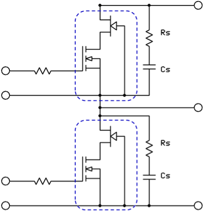
As shown in Figure 1, using a SiC cascode with a low-voltage MOSFET and a SiC JFET enables a fast cold-off device with virtually zero gate-to-drain capacitance CGD, thus partly solving the problem. can be mitigated.
External gate resistors R(ON) and R(OFF) can control the edge rate to reduce dV/dt and di/dt. This is a very practical solution and can be used to upgrade existing systems using standard Si MOSFETs and IGBTs to be more efficient while keeping the existing gate drive circuitry. Using an external gate resistor to slow down the edge rate introduces a delay between the output of the control IC and the switch gate, limiting the minimum on-time and thus limiting the control range and operating frequency. . It also slows down the response time to shutdown commands in the event of a failure. This is a serious problem for new designs that need to operate at high frequencies to take full advantage of WBG.
Achieve high-speed cascode - Qorvo UF3C SiC FET series
A recent study by Qorvo showed that by “unbraking” the SiC JFET cathode with a faster JFET and a low-value external gate resistor, a simple RC snubber was used to adequately limit the voltage overshoot. while it has been shown to improve switching speed and efficiency. Although it might seem like a simple transfer of loss from the FET to the snubber, testing has shown that the voltage limiting effect can be achieved with a much smaller snubber. JFET improvements reduce reverse recovery charge (Qrr) by 50% and reduce turn-on losses compared to UJ3C general-purpose devices.
This "FAST" device from Qorvo is part of the UF3C series and can typically be used with snubber resistors of 5-10Ω and capacitors of 47pF or less. The actual recommended value depends on the device type and final application, with circuits such as hard-switched active rectifiers and totem-pole PFCs working best. A good rule of thumb is to set the capacitor to approximately 3 times the COSS of the device. When upgrading an existing design, the snubber locations are often already present and the value using UF3C parts is typically much smaller physically and of course at a lower cost.
Figure 2 shows a comparison of total switching losses for various devices in the 1200V/35mΩ class in the TO-247 package. The UF3C120040K3S with 33Ω gate resistance, 330pF snubber, and 5Ω shows excellent results over the entire load range, and the driver can be simplified with a single Rg.
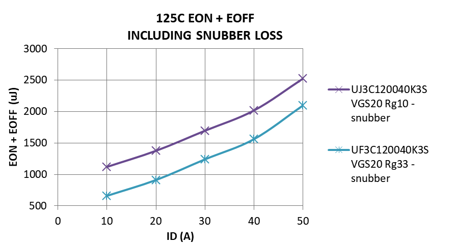
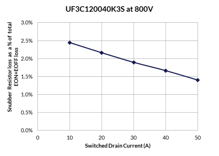
Figure 3 shows the loss measurements of the snubber resistor of UF3C120040K3S. This loss is only a small fraction of the total switching loss because the required capacitance is very small.
With the new UF3C series of SiC cascodes, you can get the efficiency benefits that high-speed switching offers without the risk of overshoot voltage stress in small snubbers. The fact that the device is compatible with a wide range of Si and SiC gate drive voltages and is also guaranteed avalanche rated is a bonus.
Inquiry
If you have any questions regarding this article, please contact us below.
Qorvo manufacturer information top page
If you want to return to Qorvo manufacturer information top page, please click below.
