
![]()
![]() Narrow down by specifying conditions
Narrow down by specifying conditions
現在1888件がヒットしています。check

Introduction
With companies like BMW, Nissan and Tesla selling capable vehicles, the shift to electric traction in cars is well underway. The benefits of such vehicles include less pollution during use and lower operating costs, but they are putting an increasing strain on the power generation and distribution grid. In the short term, utilities are responding to increased demand by increasing generation capacity or strengthening grids. In the medium term, however, the distributed storage capacity installed in a large cohort of electric vehicles will enable the grid to become smarter, and reserve battery capacity can be used to better balance the supply and demand of the grid. It may become like this. But before that can happen, we need to build a new generation of efficient on-board chargers.
Building a better charging circuit
Power grids distribute energy as alternating current (AC), while batteries store and release energy as direct current (DC). Converting between the two forms of energy delivery requires the use of circuit topologies such as half-bridge and full-bridge rectifiers and "totem-pole" configurations. To meet the charging time and efficiency requirements of on-board chargers, power factor correction (PFC) circuits must be implemented to transfer energy to and from the battery most effectively.
Evolution of power factor improvement
A switch-mode AC-DC converter rectifies the mains voltage and the resulting high voltage DC can be chopped at high frequency and converted to a lower voltage with a transformer. Bulk DC smoothing capacitors used in converters are "refilled" with charge only at the peaks of the mains voltage, so the current from the mains is far from sinusoidal. The result is a poor power factor, making it difficult for the converter circuit to drive efficiently from the mains supply. Placing a 50 or 60Hz inductor in series with these converters offers a simple PFC at the expense of increased losses and a larger circuit board (inductors can be large).
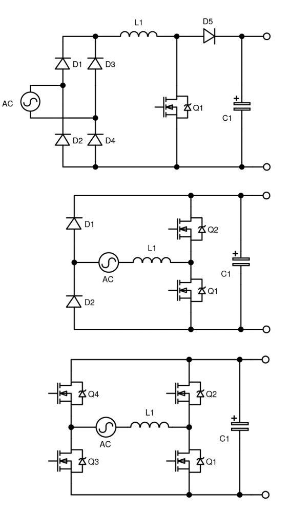
The standard alternative approach to solving this problem is to use an active switching circuit that takes the rectified mains voltage and boosts it to a constant DC level while controlling the line current to be sinusoidal. (see top of Figure 1). This approach can lead to losses at high power - the circuit topology places three diodes (D1, D4, D5 or D2, D3, D5 - depending on the polarity of the mains supply) in the current path, Each lowers the voltage and dissipates energy.
Replace diode with MOSFET
By replacing D5 with a switch similar to Q1, the circuit can be simplified such that Q1 and Q2 act as a boost switch and synchronous rectifier, alternating the polarity of the mains supply (see middle of Figure 1). ). Now there is only one diode, and the drain-to-source resistance of the switch is simply in series with the current, reducing conduction losses. The final step is to further improve efficiency by replacing D1 and D2 with synchronous switches, as shown below in Figure 1.
Manage effects of body diode behavior
As always in circuit design, there are pitfalls. Both Q1 and Q2 must always have a "dead time" in which neither conducts so that the circuit does not develop catastrophic "shoot-through" currents. During this dead time, the MOSFET's intrinsic body diode (either Q1 or Q2 depending on the phase of the switching cycle), acting as a rectifier, conducts the full output current. Reverse biasing on the next switching cycle will result in large reverse currents, causing power loss and electromagnetic interference, negating any efficiency gains. High-voltage MOSFETs have particularly poor reverse recovery characteristics of the body diode, so bridgeless totem-pole circuits are not often used for high-voltage applications.
Application of wide bandgap switch
The availability of wide bandgap switches has enabled new circuit options. SiC MOSFETs promise low channel conduction losses, high speed and fast body diodes. However, the forward voltage of the diode is 2.5-3V, leading to high conduction losses. Also, the energy stored in the device capacitance (EOSS) is typically twice that of an equivalent Si MOSFET, which increases switching losses. Some designers are using enhancement mode GaN devices because they do not have a body diode. However, the ratio of normalized die area to on-resistance RDSA is twice that of SiC MOSFETs. Also, there are no avalanche or short-circuit ratings, which raises concerns about practical reliability. Gate drive voltage is also important for reliable and efficient operation of both SiC MOSFETs and enhancement-mode GaN semiconductors.
SiC cascode option
One way to take advantage of wide bandgap devices is through the use of SiC cascodes. It combines a high voltage SiC JFET and a high performance low voltage Si MOSFET in one package. These devices are normally-off devices with defined avalanche and short-circuit ratings. These devices have extremely low input, output, and Miller capacitances, low stored energy ratings, and low switching losses, all due to their small die size. The ratio of normalized die size to on-resistance of SiC cascades is about 3-4 times higher than enhancement mode GaN or SiC MOSFETs and about 10 times higher than Si superjunction MOSFETs.
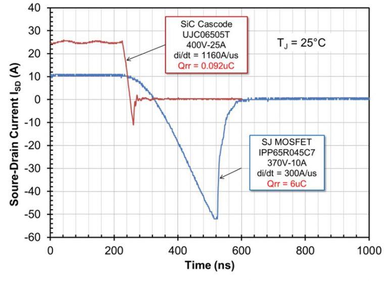
A body diode is introduced into the Si MOSFET with the SiC cathode arrangement, but because it is a low-voltage MOSFET, the operation of the diode is extremely fast, and low reverse recovery current and low loss are possible. Figure 2 compares the recovery characteristics of the 650V Qorvo UJC06505T and 650V IPP65R045C7 silicon superjunction MOSFETs, showing a ~60x difference in recovery charge.
SiC cascodes are also easy to drive, with typical operating levels of 0 to 12V and an absolute maximum of +/-25V.
Actual SiC cascode
You can explore circuit topologies and device characteristics to your heart's content, but how good is the SiC cascode for its target application, an electric vehicle on-board charger?
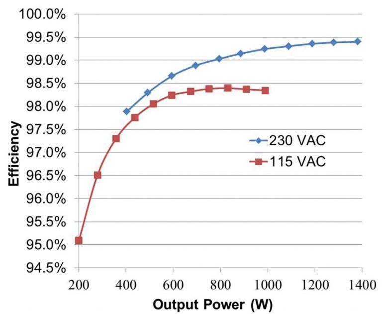
One way to assess this is to see if the complete converter meets the 80PLUS titanium efficiency standard. The standard requires converters to be at least 96% efficient at full load and half load. To meet this criterion, the PFC stage must exceed 98.5% efficiency while the main conversion stage meets the stringent requirement of 97.5% efficiency. A Qorvo 1.5kW demo board using a UJC06505K SiC cascode operating at 100kHz was found to meet this requirement with some margin (shown in Figure 3).
Realization of a bi-directional grid with EV chargers
In other words, the rise of electric vehicles is creating an opportunity to both sink and source power using a large number of energy storage units (i.e., car batteries) distributed widely across the power grid.
Making this a reality requires imagination and an on-board charger that can support energy transfer in either direction. The totem pole PFC stage described above makes this possible. If we look again at the schematic at the bottom of Figure 1 and think of the DC bus as the power source and the AC line connection as the load, then, with proper driving of the MOSFETs, we have a half-bridge inverter circuit that transfers power from the DC battery back to the AC source.
With the spread of electric vehicles, using SiC cascode for PFC improves the efficiency of on-board chargers. It may also be used to increase the capacity and efficiency of the power grid itself due to its robustness and adaptability.
Inquiry
If you have any questions regarding this article, please contact us below.
Qorvo manufacturer information top page
If you want to return to Qorvo manufacturer information top page, please click below.
