
![]()
![]() Narrow down by specifying conditions
Narrow down by specifying conditions
現在1887件がヒットしています。check

Introduction
Nothing beats the laws of physics. Resistors release electrical energy as heat and as a voltage drop. Capacitors take time to store charge and take time to release charge. Inductors take time to generate and collapse electromagnetic fields. Since there is nothing we can do about it, electronics designers have learned to avoid these factors by developing clever circuit topologies since the days of thermionic valves. Physics is physics, and what worked for valves turned out to be equally applicable to today's high-performance semiconductors.
How Mirror Capacitance Limits High Frequency Amplification
For example, consider the mirror effect. In the 1920s, American electrical engineer John Milton Miller identified a problem with simple triodes when used as amplifiers due to the internal capacitance between the grid and anode. This capacitance reduced the bandwidth of the amplifier by increasing the amount of negative feedback, as the impedance of the capacitance decreased with increasing operating frequency.
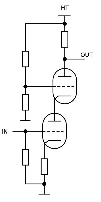
Miller realized that connecting two triodes in series (CASCaded triODE, or cascode topology) as in Figure 1 reduced the total capacitance from input to output. If the upper tube grid is fixed voltage, the cathode voltage of the upper triode is controlled by the lower triode. When tetrodes were developed with internal screens, this internal capacitance and its associated effects were reduced, making it possible to build single-tube amplifiers operating at hundreds of megahertz.
Restoration of the mirror effect
The Miller effect returned when designers began replacing thermionic valves with solid-state semiconductors, which again began to limit high-frequency operation.
Why did that happen? In MOSFET-based switching circuits, the Miller effect limits switching speed because the drive circuit must charge and discharge the input capacitance in a reliable and low-loss manner. The effect of this Miller capacitance, called CGD, depends on the gate voltage.
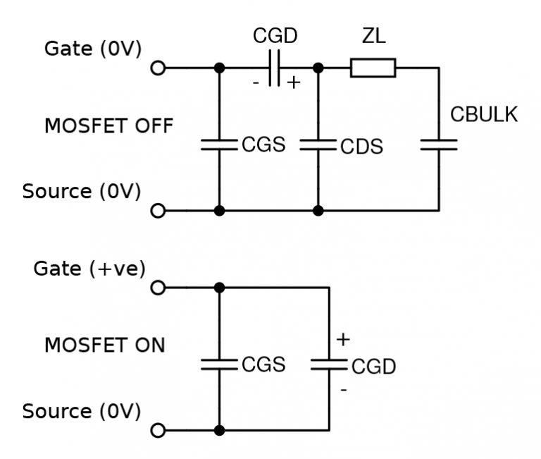
For example, consider an enhancement-mode MOSFET switch that turns off when its gate is at 0V. The total gate input capacitance is shown as a network including CGS, CGD, CDS, load ZL, and bulk (see Figure 2). There is also a positive voltage across the capacitance CBULK, CGD. When the MOSFET turns on, the drain voltage drops to almost zero, the total capacitance is CGD in parallel with CGS, and there is a negative voltage across CGD compared to the off state. When switching from on to off and back, the input capacitance must be switched back and forth between these conditions.
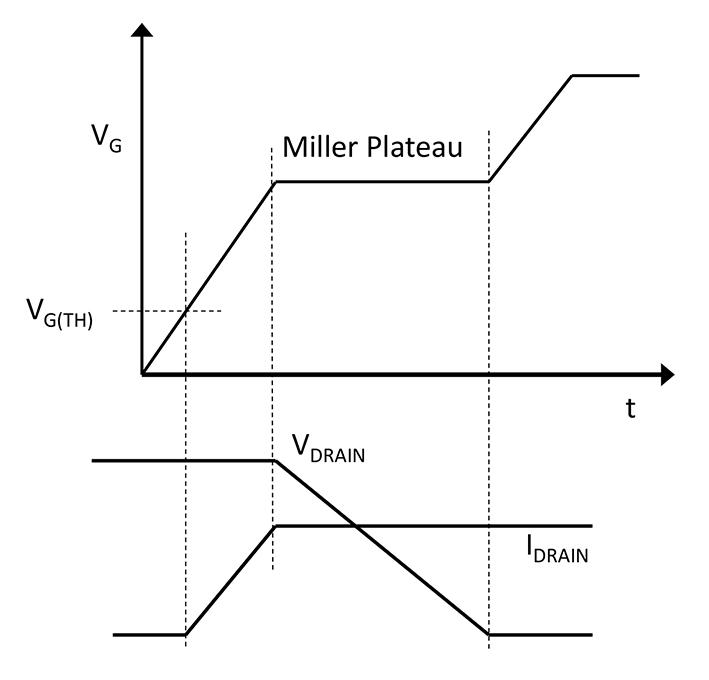
The plateau in the positive-going portion of the MOSFET gate switching waveform (see Figure 3) represents the transition between the two input capacitance states, the driver must act sharply, and the switching transition will be late. Worse, when the voltage on the drain drops, it tries to make the gate negative through CGD against the positive turn-on voltage command. When turning off the MOSFET, this process is reversed when driving the MOSFET off. Because CGD tries to "pull" the positive voltage on the gate, designers using MOSFETs and IGBTs are encouraged to use a negative off-state gate voltage to combat this effect. This increases the power required to drive the gate.
Gate/drain capacitance control
A device's gate-drain capacitance (CGD) is affected by the semiconductor device's architecture and therefore varies depending on whether it is placed horizontally or vertically. For low-voltage MOSFETs, it is possible to minimize CGD, but at higher voltages, especially when one wants to build wide-bandgap devices using materials such as silicon carbide (SiC) and gallium nitride (GaN). It can be a problem. The switching speed of these technologies is limited by Miller capacitance, and the best way to combat this effect is to use a cascode circuit topology.
modern cascode
A basic SiC switch employs a junction FET (JFET) architecture. Configuring the JFET as a vertical device results in a lower CGD and a lower drain-source capacitance CDS. However, the JFET is a normally ON device with a 0V gate and requires a negative gate voltage to turn it OFF. This is a bridge circuit problem that causes all devices to default to the ON state the moment they are powered up. Such a circuit would be better off using a normally-off device by arranging a Si MOSFET and a SiC JFET in a cascaded topology (Figure 4).
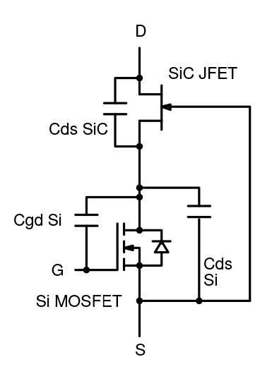
When the MOSFET gate and source go to 0V, the drain voltage rises. The gate of the JFET is also 0V, so if the drain to source voltage of the MOSFET rises to 10V, the JFET will have a negative voltage of -10V between the gate and source and will turn off. Since the MOSFET gate turns on when it goes positive, short the gate-source of the JFET to turn it on. This circuit topology creates a "normally-off" device. This topology also allows the series input/output capacitance to include the JFET's CDS, which is close to zero, thus reducing the impact on the Miller effect and high-frequency gain.
Other benefits
During switching, the Si MOSFET drain voltage "pots down" the JFET drain voltage because the JFET drain-source capacitance CDS is nearly zero and the MOSFET CDS is non-zero, so the MOSFET drain voltage is remains at low voltage. This allows the MOSFET to be a low-voltage type with very low drain-to-source on-resistance and much easier gate drive characteristics. In addition, the low-voltage type MOSFET body diode has the advantage of very low forward drop and fast recovery. JFETs do not have a body diode, so the body diode of the MOSFET conducts when reverse switch conduction in the 3rd quadrant is required, such as in a rectifier bridge circuit or synchronous rectification. This clamps the JFET's gate source to about +0.6V to ensure a hard on and reverse current flow with a low voltage drop.
end of mirror effect
The SiC cascode topology solves the Miller capacitance problem, provides easy gate drive, normally-off operation, and a high performance body diode. This is different from SiC MOSFETs, which tend to have poor body diode characteristics, and GaN HEMTs, which tend to have high CDS. The invariants of physics that led to the high-frequency gain-limited Miller effect in thermionic devices also apply to semiconductor devices. But this invariance of physics means that cascode-based solutions work just as well in modern SiC devices as they do in classic valves.
Inquiry
If you have any questions regarding this article, please contact us below.
Qorvo manufacturer information top page
If you want to return to Qorvo manufacturer information top page, please click below.
