
![]()
![]() Narrow down by specifying conditions
Narrow down by specifying conditions
現在1888件がヒットしています。check
Maximizing Photovoltaic Solar Energy Efficiency with SiC Semiconductor Three-Level Inverter
The economics of large-scale solar power plants are based on selling energy to the power grid for a profit. Energy conversion efficiency and equipment cost are critical determinants of viability and are influenced by the design choices that shape the inverter and associated power conditioning electronics. Silicon carbide technology promises significant efficiency gains, but other factors must be considered, such as the total number of power devices required and associated conduction/switching losses, device size and cost for rated voltage. not.
Inverters typically require a DC/DC converter at the input capable of either step-down or step-up operation to ensure a stable DC-link voltage even if the panel output fluctuates. The topology of the inverter influences the design of the DC/DC converter circuit and greatly affects the number of power switches required and BOM cost.
A basic 6-pack 3-phase inverter consists of three high-side and low-side transistors, which may seem like the simplest and lowest-cost solution, but this arrangement allows the AC neutral and the DC input is known to generate four steps of common-mode voltages with the same amplitude as the DC-link voltage. In large solar farms this can lead to unacceptable leakage currents in the DC link. If the inverter specification calls for isolation, transformers effectively prevent the flow of these leakage currents, but if isolation is not required, introducing a dedicated compensating transformer would result in unnecessary additional cost and bulk will occur.
By using a 3-level inverter topology, the common mode voltage and thus the leakage current can be dramatically reduced without the need for additional transformers. Neutral point clamp (NPC) or transistor-type neutral point clamp (TNPC) topologies are usually considered. Losses increase due to the need for extra switches, the associated drivers further increase the BOM cost, and controlling the inverter becomes a more complex challenge. On the one hand, the designer has the freedom to optimize the overall cost and performance of the inverter through device selection.
Choices in practical applications
Consider a 50kVA generator designed to have a nominal DC link voltage of 800V, an input voltage booster of 300-800V, and an operating frequency of 25kHz. Figure 1 compares the number of power switches required to build such a converter/inverter using standard two-level or three-level inverter topologies. The design is based on power loss analysis and uses paralleled switches to keep the junction temperature below 25°C. Power loss analysis assumes no electrical isolation between the semiconductor and the heat sink.
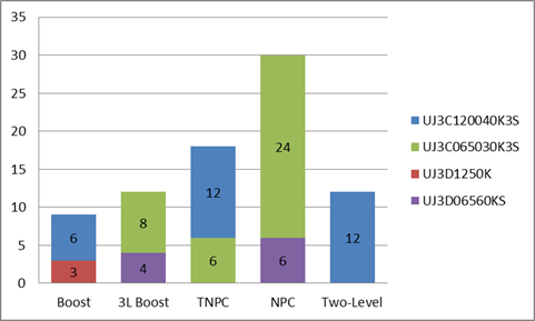
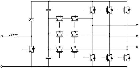
The TNPC circuit consisting of 12 UJ3C120040K3S 1200V SiC cathodes and 6 UJ3C065030K3S 650V SiC cathodes seems to be the winner considering the total parts count. Figure 2 shows a sample schematic consisting of a TNPC at the input and a suitable booster.
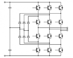
A diode-clamped NPC circuit (Figure 3) has more semiconductor components than a TNPC. As can be seen from the power analysis in Figure 1, the NPC inverter consists of 24 UJ3C065030K3S SiC cathodes and 6 UJ3D06560KS SiC Schottky diodes, while the TNPC circuit has 18 cathodes. However, the NPC can be built using only 650V devices, realizing the strength of this topology, the high DC link voltage compared to the component ratings.
If the DC link voltage is 800V, TNPC requires a 1200V switch to avoid single event burnout (SEB) of power devices. The arguments in favor of NPC inverters and 3-level boosters are compelling when reliability models require a generous voltage margin or when DC link voltages of 1000V or higher are required.
SiCカスコードの利点
Using Qorvo cascodes in inverter and booster circuits provides additional benefits in addition to improved energy efficiency, thermal endurance, and die size tolerance. In inverters, the SiC semiconductor FET UJ3 series cascodes can be held at as little as 10V or less, which helps ensure sufficient holdup time when bootstrapped gate drive supplies are used. To achieve fast switching, the gate voltage should be +15 to 18V at turn-on and -5V at turn-off.
Additionally, using cascodes instead of diodes in boosters means that booster plus inverters can handle power in two directions. The cascode can act as a switch or a diode depending on the direction of power flow, so the system acts as a DC-AC inverter or AC-DC active front-end rectifier. Since the heat load varies between inverter and rectifier modes, the number of devices should be the same in each switch position of the booster.
Overall, the combination of high energy efficiency, robustness, and fast switching performance makes SiC cascodes ideal for switching frequency, DC-link voltage, reliability, and BOM in systems using two-level or three-level booster/inverter topologies. It offers designers the flexibility to control costs. TNPC inverters are usually preferred when using a three-level topology to minimize common-mode voltage in non-isolated designs. The NPC topology is a strong choice when higher input voltages are required.
Inquiry
If you have any questions regarding this article, please contact us below.
Qorvo manufacturer information top page
If you want to return to Qorvo manufacturer information top page, please click below.
