
![]()
![]() Narrow down by specifying conditions
Narrow down by specifying conditions
現在1888件がヒットしています。check

Wide Bandgap Devices - What These Devices Promise
Wide bandgap (WBG) semiconductor technologies such as Silicon Carbide (SiC) and Gallium Nitride (GaN) are hot topics at the moment, shrinking in size in most applications, from universal wireless charging to power converters. A device that promises However, choosing the available technologies and devices is not always easy, and the markets they can penetrate are wider than you might think.
Let's take a step back and outline what a WBG device is. Semiconductors have bonding electrons that occupy different energy levels (valence and conduction bands) around the nucleus. Electrons can move up to the conduction band and conduct current, but they need energy to do so. For WBG devices, this energy requirement is much higher than for silicon (Si). For example, SiC requires 3.2 electron volts (eV) compared to Si at 1.1 eV. The increased energy required to transfer electrons to the conduction band in WBG devices translates to higher field breakdown performance compared to Si of the same scale. For the same reason, SiC can withstand high temperatures (thermal energy) before failing, and as a material it has about 3.5 times the thermal conductivity of Si. In practice, these attributes promise high frequency, high temperature operation at high voltage and power levels.
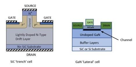
The first devices available in SiC were simple diodes, but materials technology has advanced to allow the fabrication of JFETs and MOSFETs. Figure 1 shows a SiCJFET cell with a vertical trench structure that gives a very low on-resistance compared to a GaN high electron mobility transistor (HEMT) cell with a lateral structure.
Find the best solution for your application
Enhancement-mode, normally-off, Si- and now SiC-MOSFETs are the best components for low- and medium-power switching applications, but they have some drawbacks.
• The MOSFET has an integral body diode with high forward voltage drop and relatively high recovery charge (Qrr). This is usually changed by a factor of 3 overheating. High Qrr and high forward voltage drop cause high losses in circuits that force or conduct body diodes, such as choppers, hard-switched bridges with inductive loads, and bridgeless totem-pole circuits for PFC stages. An additional parallel SiC Schottky diode can be added to bypass the body diode, but at considerable cost and of limited benefit.
• For MOSFETs, the gate turn-on threshold is low, for example around 2.2V for SiC devices, but the gate-source voltage must be kept within very tight limits for optimum and safe performance. there is.
• Short-circuit saturation current varies with gate-source voltage and is poorly controlled, which is a major concern for system reliability.
• Input, output and Miller capacitance around the MOSFET are relatively high. This leads to significant gate drive power requirements, losses as the capacitance is charged and discharged, and the risk of spurious device turn-on from current injected into the gate via the Miller capacitance.
A JFET can be considered without a body diode, but typically turns on when the gate voltage is zero and turns off when about -7V is applied. Normally-on devices are useful in some applications such as circuit breakers, but normally-off types are much preferred in switch applications.
Cascode connection of switches
To avoid the MOSFET problem while using WBG technology, manufacturers went back to 1930s tube technology and revisited the cascode connections shown in Figure 2.
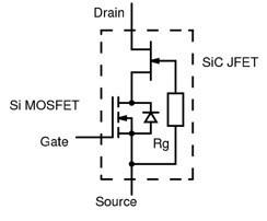
Here, a low-voltage Si-MOSFET is connected at its drain to the source of the SiC trench JFET, and the JFET gate is connected to the MOSFET source. Applying a positive voltage to the Si-MOSFET gate turns it on, effectively shorting the gate and source of the JFET to turn it on. When the Si-MOSFET gate is at zero volts, it turns off and the voltage at the drain rises.
However, when this reaches about +6V, the JFET gate becomes 6V more negative than the source and turns off. The drain voltage of the MOSFET increases to 15-20V based on the voltage required to fully pinch off the JFET. Unlike other cascode implementations, the nearly zero CDS of the JFET after pinch-off means that the capacitive voltage divider with the Si-MOSFET dominates any voltage developed across the HVJFET. Masu.
SiMOSFETs can therefore be of the low voltage type with a very low on-resistance RDS(on) of a few milliohms. In that case the overall on-resistance is dominated by the JFET channel. Now you have a normally off device like a MOSFET, but as a bonus you also solved the limitations of other MOSFETs.
• Body diodes have been introduced as part of low-voltage Si-MOSFETs, but they are more than two times smaller than high-voltage SiCMOSFETs and have very low Qrr figures, on the order of 20 times that of standard fast-recovery diodes. . A practical circuit in which the body diode conducts does not require an extra parallel diode.
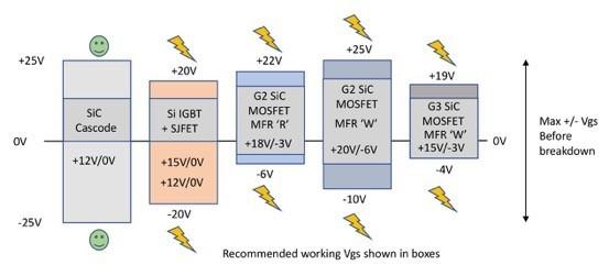
• Si-MOSFET gate drive is not critical compared to SiC-MOSFET and can withstand up to +/- 25V.
• The cascode Si-MOSFET gate-source voltage is about +8V and has no effect on the short-circuit saturation current after full enhancement. Current is now controlled by a "pinch-off" effect within the JFET's vertical trench, which effectively limits the current to the saturation level. Furthermore, the heating effect caused by the current reduces the conductivity of the JFET channel, giving it self-limiting properties. A higher junction temperature tolerance also helps in this regard.
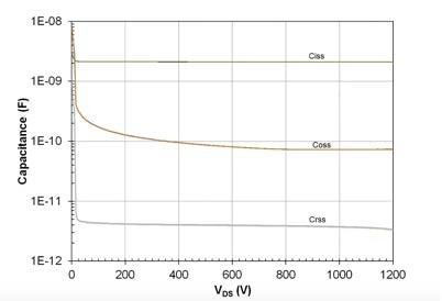
• Si-MOSFET in cascode is low voltage and optimized for application, so its input capacitance Ciss is low, cascode drain gate. Miller capacitance Crss is practically zero. See Figure 3 for the Qorvo 1200V 60mΩ device. This reduces the gate drive power and eliminates the risk of spurious turn-on due to positive dV/dt on the drain pushing current spikes through the Miller capacitance into the gate drive circuit.
• There is switching associated with Coss, energy lost in Eoss. For 650V class devices, SiC cascodes of about 6.5µJ have more than half the value of comparable Si- or SiC-MOSFETs.
If there is a caveat with cascode, it needs to be slowed down. Practical designs limit dV/dt and di/dt to manageable values to meet EMC standards and limit induced current spikes in associated circuits and voltage spikes across connection inductances. With careful configuration, the cascode configuration allows effective control of dV/dt and di/dt using external gate resistors.
Figure 4 shows the observed values for gate resistance R(on) between 2.35 and 20.5 ohms for UnitedSiC UJC1206K cascode devices with a 600V inductive load. Note that every 1nH of inductance produces a 1V transient with a di/dt of 1000A/µs. When this transient appears in the gate circuit loop, it reduces the turn-on or turn-off margin. Similarly, an easily achievable 50V/ns dV/dt produces a 1A current spike with only 20pF of stray capacitance.
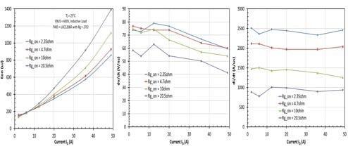
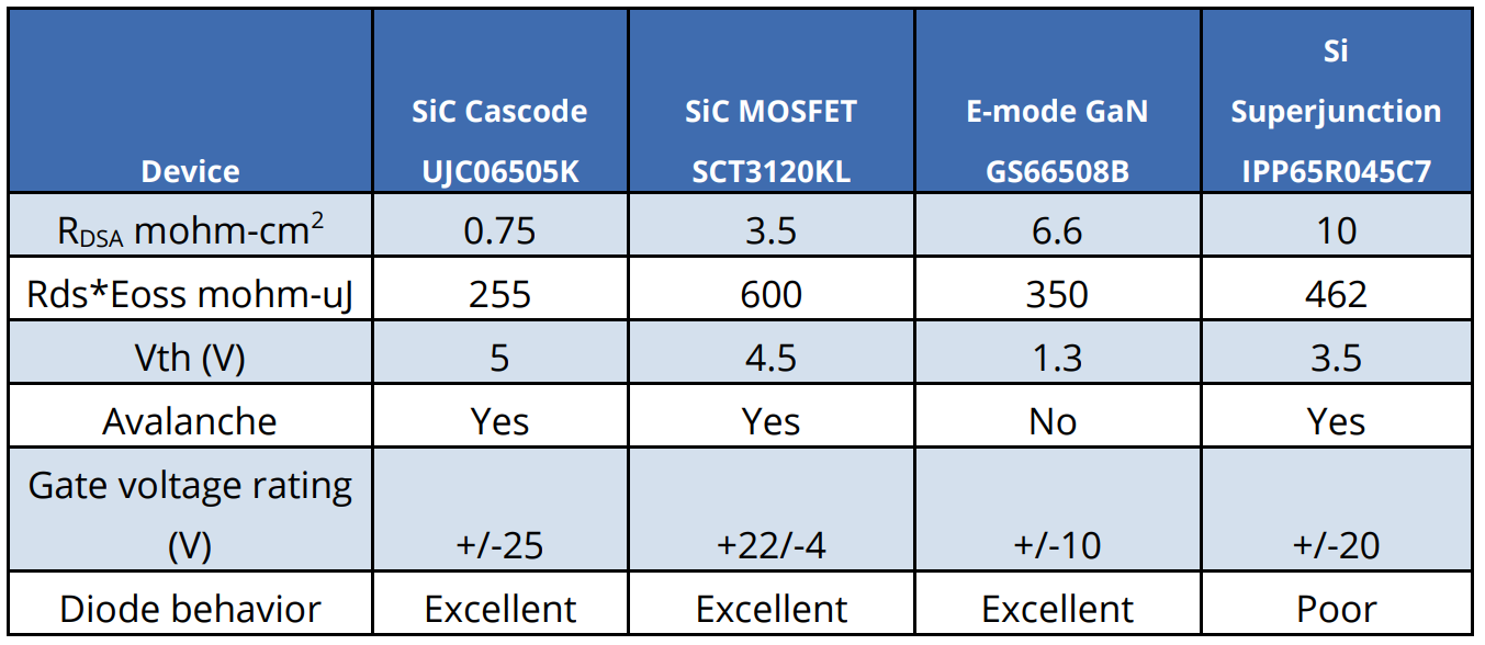
Figure 5 summarizes the mutual characteristics of WBG technology and the relative characteristics of conventional Si superjunction MOSFETs.
Cascode "drops in" to existing applications
The main advantages of WBG devices are often seen as speed and high temperature operation at several MHz and junction temperatures in excess of 200°C, promising dramatic reductions in size and cost along with increased efficiency. This is definitely possible with a ground-up redesign using new magnetics, resonant topologies and RF-style layouts. Perhaps the best example is the Google and IEEE "Little Box Challenge" to design a 95% efficient converter with a power density of 50W/in3, one-tenth the state-of-the-art version at the time. The winner uses WBG technology to achieve better than 145W/cu-in.
However, there is a vast market for upgrading existing equipment, and a complete redesign is neither feasible nor economical. Most WBG switch solutions are not suitable for engineered components such as IGBTs and Si-MOSFETs. The gate drive systems for these components are not compatible with the exact gate drive voltages required for SiC-MOSFETs, GaNHEMT devices, etc. However, cascode SiCJFETs are ready to drop-in. Can be used with conventional TO-247 and TO-.
The 220 case style can accept a wide range of gate drive voltages, including all other device standards (Figure 6). Some cascodes also include gate clamp diodes to protect against overvoltages and ESD. The gates of IGBTs and Si-MOSFETs in existing systems are often driven directly through transformers with imprecise voltages that vary with duty cycle. Again, the wide gate voltage drive tolerance for the SiC cascode makes replacement easier.
Cascode can be slowed down by choosing gate resistors to match existing designs, dramatically reducing body diode energy losses compared to Si-MOSFETs and IGBTs with external fast recovery diodes To do.
System stability and potential speed are improved, the Miller effect is virtually eliminated, and gate drive power is significantly reduced. As an example, comparing the SiC cascode of Qorvo type UJC1210K 800V/20A with the IGBT type IRG7PH35UD600V/25A, the total gate charge QG (total) of the cascode is 47.5nC, IGBT85nC. This may not seem like a big difference, but even if the IGBT requires 9V/+15V, the cascode can switch to 0V/12V at the gate. The gate drive power requirement PG is given by:
PG = QG (total) × F × VSW
where F is the operating frequency and VSW is the total gate voltage swing, twice the cascode value for IGBTs. So the total power required is about 4 times less with a cascode connection. Note that the power remains constant for any duty cycle as long as the gate is fully charged and discharged in each switching period.
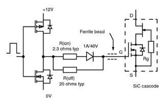
SiC cascodes can therefore be dropped into many applications using IGBTs, SiMOSFETs or SiC-MOSFETs, simply changing the series gate resistance value to optimize switching speed. A typical gate drive circuit for SiC cascode is shown in Figure 7. R(on) is typically lower than R(off) and should be a minimum of about 10 ohms to avoid internal cascode oscillations. A series ferrite bead is an option for damping.
SiC vs GaN
GaN, which appeared later than SiC, has been slow to adopt due to issues of cost, yield, and reliability. Theoretically, higher switching speeds than SiC and Si are possible, and electron mobilities are much higher, but thermal conductivity is one-third lower than SiC, which limits power density potential. . SiC devices are now common with ratings around 650V to 1.2kV and above, while GaN is limited to around 650V, competing with the current low cost and proven robustness of more mature SiC products at the same voltage. I am struggling with
GaN suppliers hope that low voltage/power markets such as data centers, EV/HEV, and solar power will open up as the expected cost savings are realized. However, SiC cascodes also address these market areas, especially in bidirectional DC-DC converter and totem pole PFC applications (see below). IHS data shows that the relative split of usage will remain the same through the mid-2020s, with the WBG market totaling $3.5 billion, of which GaN is still around $500 million.
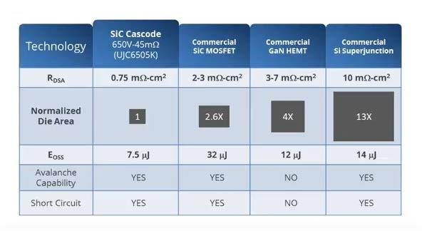
SiC is now well established in the supply chain and parts are available in high service distributor catalogs. SiC trench cascodes have an advantage over GaN, indeed Si-MOSFETs and SiC-MOSFETs, in that they have a much better figure of merit RDSA (Figure 8). RDSA is a measure of the combination of ON resistances achieved in a given die area, and comparing the same power levels between devices, SiC cascodes, for example, outperform GaN by a factor of 5-10. In other words, the die size can be reduced by a factor of 5-10, resulting in less capacitance, more die per wafer, and associated cost savings. Although it has a smaller heat transfer area, SiC has three times the thermal conductivity of GaN and can withstand junction temperatures up to 250°C with little change in properties anyway.
Perhaps even as GaN voltage ratings improve to compete, the factor that gives SiC its edge in industrial systems is its ability to withstand voltage avalanche conditions that can occur with inductive loads. Manufacturers have extensive data showing the reliability overvoltage overstress of SiC, but GaN makes no claims except that the maximum voltage should not be exceeded.
A more specific difference between devices is the packages available. SiC parts are commonly available in TO-247 and T0-220 styles and can be drop-in replacements for MOSFETs and IGBTs in existing designs, providing immediate benefits. Various standard surface mount options are under development. However, GaN device manufacturers recognize that leaded packages with their inherent rate-limiting connection inductance are a barrier to getting the best potential performance from their parts.
Therefore, they have mostly opted for surface-mount, single-source, chip-scale packaging, limiting their adoption to new designs. Here, system designs can be adapted to the properties of GaN devices to give smaller passive components, especially magnetics and capacitors.
Current WBG device position
SiC cascodes are commonly available in ratings of 650V and 1200V with currents up to ~85A and on-resistances of ~30mΩ. As introduced in a previous article, a "super-cascode" is also available (series-connected JFETs rated above 3.5kV). SiCMOSFETs up to 1700V at about 70A and 45mΩ are available, but their internal body diodes, unlike cascodes, are relatively slow and can be bypassed with, for example, an expensive and fast SiC external diode if the application requires it. is needed.
GaN devices are rated at about 60A and 25mΩ at 650V, comparable to many SiC parts, but theoretically capable of switching faster. Interestingly, GaN devices available with a 100V rating do not outperform conventional Si-MOSFETs in terms of on-resistance, thus countering the significant cost over commodity MOSFETs at this level. We rely on the speed advantage for that.
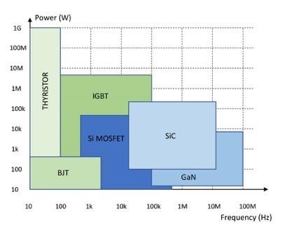
Looking ahead, IHS data clearly show a significant increase in WBG device design-ins, while IGBT and conventional MOSFET sales will also increase in the growing market. The question is how different WBG devices dominate specific market segments. Figure 9 is one view of the potential future partitioning of power and operating frequency for power devices, but the existence of GaN depends on the expected cost reductions.
application
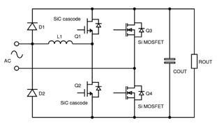
The high temperature capabilities of WBG devices with potentially fast switching and low losses make them ideal for military and industrial applications where performance is critical. Bridge circuits are obvious candidates for high power applications such as inverters, welding, class D audio amplifiers, and motor drives. A particular application that sees major benefits is the bridgeless totem-pole PFC circuit (Figure 10).
Here, previous circuits using Si technology were limited by the slow performance of the body diodes of the commonly used MOSFETs. SiC diodes in parallel help, but defeat the goal of reducing component count. This forces the use of the “critical conduction” mode, setting the switching current to zero at the end of each conduction period. However, this variable frequency mode produces high peak currents and high EMI. Cascode SiCJFETs allow the use of a “continuous conduction” mode to increase efficiency, reduce inductor size, and alleviate filtering and EMI issues at fixed operating frequencies. An example circuit using the Qorvo UJC06505K device on a 1.5kW and 230VAC line showed an impressive efficiency of 99.4%.
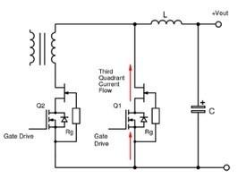
Achieving high efficiency in the converter's primary switch must be matched by similar improvements in DC output rectification. Again, SiC cascodes fit here because they can be configured for "synchronous rectification" (Figure 11). In so-called 3rd quadrant operation, current flows from the source to the drain of one of the cascodes through the output inductor to load it during the "forward" and "flywheel" periods of a forward or buck converter.
The current through the body diode sets the JFET's gate-source voltage to about +0.7V, naturally turning it on hard. When the cascode gate is set high, the internal Si-MOSFET channel conducts and the total ON resistance is the RDS(on) of the cascode, resulting in low conduction losses. Q1 forms a flywheel rectifier and Q2 forms a forward rectifier.
Robustness concerns
Robustness to transient short circuits and overvoltages is a major concern in high power applications. A typical cascode SiCJFET has excellent properties in this regard. The pinch-off effect was already mentioned, but the saturation current is limited by a negative temperature coefficient.
In case of overvoltage, the SiC JFET gate-drain diode conducts, allowing current to flow through the internal gate resistor, turning on the JFET channel and clamping the overvoltage. Again, the SiC die's inherent high temperature rating provides a sufficient safety margin for significant avalanche energy levels, even at relatively small die sizes. As an additional measure of reliability, all parts are subjected to 100% avalanche area in final testing.
Inquiry
If you have any questions regarding this article, please contact us below.
Qorvo manufacturer information top page
If you want to return to Qorvo manufacturer information top page, please click below.
