
![]()
![]() Narrow down by specifying conditions
Narrow down by specifying conditions
現在1888件がヒットしています。check

Current status of SiC device and package technology
It has long been known that packaging technology is critical to unlocking the potential of wide bandgap (WBG) devices. Silicon carbide device manufacturers are rapidly improving device technology figures of merit such as on-resistance per unit area (RdsA) while simultaneously reducing parasitic capacitance for faster switching. A new package has been released that allows users to take better advantage of the WBG fast switching performance. Standard modules are becoming more available and new switching technologies are being applied to increase the value of products with faster switching speeds, improved thermal resistance and improved reliability.
device technology
SiC Schottky diodes account for more than 50% of SiC sales, mainly in the 650V, 1200V and 1700V classes. 650V diodes are used in power factor correction circuits (PFC) in computer, server and telecom power supplies and secondary rectifiers in high voltage battery chargers. 1200V and 1700V diodes are used in a wide variety of circuits like solar boost circuits, inverters, welding, and industrial power supplies.
SiC Schottky diodes significantly reduce QRR compared to silicon fast recovery diodes, resulting in reduced EON losses for switches in half-bridge or chopper circuits operating in hard-switched continuous conduction circuits. Most manufacturers offer JBS diodes because pure Schottky diodes have weaknesses under avalanche and forward surge conditions. Add a PN junction to join Schottky, shield from high surge voltages, reduce leakage current and improve avalanche robustness. A PN junction bipolar reduces the forward voltage drop caused by surge conditions.
SiC diodes generally have much higher surge immunity than silicon fast recovery diodes. This is mainly due to the small forward voltage developed under surge conditions. This is only 1-2 V for silicon, but 4-6 V for SiC-FETs. However, since SiC diode dies are very small, this poses a thermal problem.
Manufacturers have used wafer thinning to reduce the on-state forward voltage and reduce thermal resistance. Advanced die attach schemes for TO and DFN packages, such as silver (Ag) sintering, are used to minimize thermal resistance and prevent melting under surge conditions such as seen in traditional solder joints . This can provide about 8-12 times more surge capability than the rated current. In terms of yield and current rating, Qorvo uses 100A, 1200V and 200A, 650V diodes for power modules. A wide range of Ag-sintered (Pb-free, green) diodes are offered and are AEC-Q101 qualified to permit use in automotive applications.
SiC transistor technology
Figure 1 shows the key device structures that dominate the market for 650V high performance FETs for power conversion. Of these, gallium nitride (GaN) HEMTs (High Electron Mobility Transistors) are the only planar devices with both power terminals on the top side of the wafer. Silicon superjunction devices have effectively zero charge with equal doping of the N-type and P-type columns and use the charge balance principle to maintain voltage even when the N-type column is heavily doped for low resistance. allows rapid depletion for
Between 2000 and 2018, adding more N-type columns per unit area reduced the on-resistance to nearly 10 times less than conventional silicon without charge balancing. Silicon superjunction technology accounts for $1 billion in annual sales, and products with on-resistance per unit area (RdsA) values as low as 12-18 mΩ-cm2 are on the market. 8mΩ-cm2 can also be achieved.
GaN HEMTs now have excellent switching behavior, with RdsA currently in the range of 3–6 mΩ-cm2. These are planar devices built on silicon substrates, which are much cheaper than SiC substrates, but today GaN devices are still more expensive than Si devices. 650V SiC trench and planar MOSFETs are also available with RdsA in the 2-4mΩ-cm2 range. Qorvo's second generation trench JFET (UJC06505K) achieved an RdsA value of 0.75 mΩ-cm2.
This means SiC JFET dies can be 1/7th to 1/10th the size of silicon and thus much smaller than GaN or SiC MOSFET structures. This is very important information if the designer's goal is to achieve cost parity with silicon.
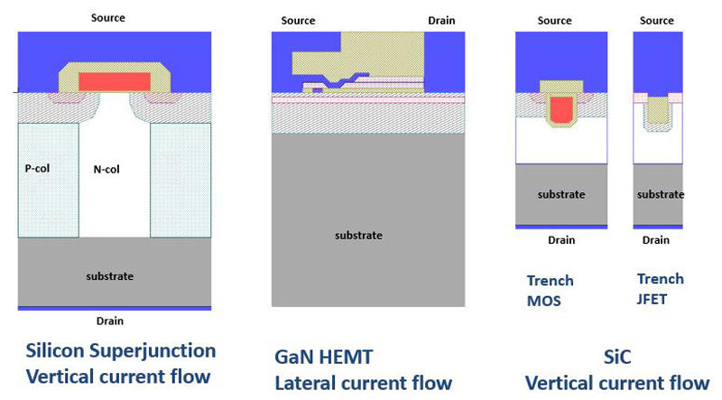
Figure 1: Device architectures most commonly used for 650V transistors of silicon superjunction, GaN HEMT, silicon carbide (SiC trench MOSFET) and SiC trench JFET (junction field effect transistor)
Most power devices are trench type to provide space for high current electrodes. GaN HEMTs are planar and have both power electrodes on the top surface.
Qorvo's FETs use a cascode structure, as shown in Figure 2, where a low-cost 25V silicon MOSFET is packaged together with a normally-on SiC JFET to create a normally-off MOSFET, IGBT, or It is a device that can be used to replace SiC MOSFETs. The device also works well in freewheeling diode mode and does not require the anti-parallel silicon fast recovery diodes used in Schottky diodes in IGBTs or SiC MOSFETs.
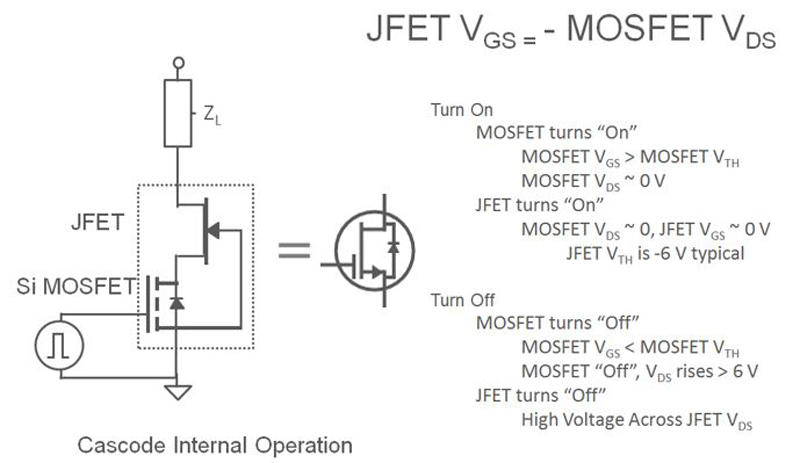
Figure 2: Inside the Qorvo cascode FET, a 25V silicon MOSFET is packaged with a SiC JFET to provide normally-off operation, simplified gate drive, and excellent body diode behavior.
The device can be dropped into existing silicon MOSFET and IGBT sockets and can be used interchangeably with all types of SiC MOSFETs.
Figure 3 compares the structures of IGBT, SiC MOSFET and trench JFET. The IGBT is a bipolar device that turns on at a knee voltage of 0.7V, after which charge carrier injection reduces the resistance of the wide voltage blocking layer. To return the device to the blocking state, these carriers must be removed, inevitably causing "switching" losses. This is much higher than the losses encountered in SiC MOSFETs.
In contrast, Qorvo's cascode can directly replace silicon carbide per unit area and improve efficiency. As explained in Advantages of SiC Semiconductors, the lack of knee voltage in the conduction of SiC MOSFETs and SiC Cascode FETs improves efficiency even in low frequency applications.
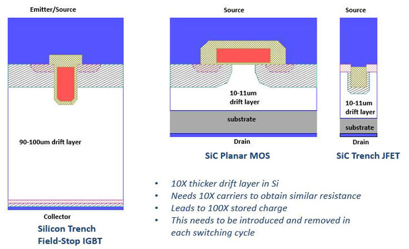
Figure 3: Above 1200V, the most commonly used silicon device is the fieldstop IGBT
SiC MOSFET and SiC trench JFET structures are shown side by side. SiC devices use 10 times thinner voltage blocking layers with 100 times higher doping levels, enabling lower resistance. Silicon IGBTs lower their resistance by injecting stored charge in the on-state. It must be added and removed on each switching cycle.
Figure 4 details the various SiC transistor offerings currently on the market. Most suppliers offer SiC planar MOSFETs, but some have introduced trench MOSFETs. All SiC MOSFETs suffer from poor in-channel mobility (about 15-30 times worse than silicon), but trench MOSFETs are better due to the crystallographic orientation of the channel. Trench JFETs have a bulk channel with much higher mobility, resulting in lower resistance per unit area for devices rated between 650V and 1700V.
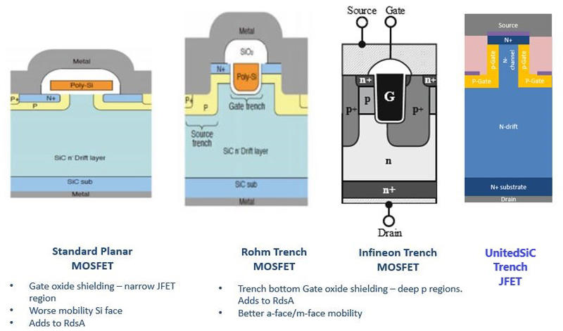
Figure 4: Device structures for SiC planar and trench MOSFETs and SiC trench JFETs
A MOSFET has a channel that is induced under the gate oxide by a voltage applied to the gate. The JFET channel exists with no voltage and is pinched off by reverse biasing the gate-source PN junction. The low resistance of trench JFETs comes from the bulk channel, without the need to shield the gate oxide from high electric fields.
SiC devices typically operate at field strengths ten times that of silicon devices. This can be constructed with a drift layer that is ten times thinner or less. While this is not an issue in bulk channel devices such as JFETs, it is important to reduce the oxide thickness of MOSFETs to avoid levels of stress on the oxide that reduce operating lifetimes or cause excessive failure rates. / Care must be taken with SiC connections. Both planar and trench JFETs inevitably further increase the on-resistance if the gate oxide is shielded to control this area.
SiC JFETs have very low resistance, the SiC substrate on which the device is built contributes more than 50% in the 650V class and 30-40% in the 1200V class. For this reason, the wafers are thinned from an initial thickness of 350um to 100-150um and can be formed by Qorvo's patented method of laser contacting from the backside.
Extending this technology and improving the cell design is expected to further reduce the on-resistance to 0.5mΩ-cm2 at 650V and 1.0mΩ-cm2 at 1200V. SiC cost reductions driven by rapidly expanding demand may therefore be further boosted by these technological improvements. Most production today is done on 6 inch wafers, with 8 inch efforts starting. Devices with ratings from 100A to 200A are now available.
Qorvo currently produces 9mΩ, 1200V stacked cascode chips (5.7x6.3mm) and 5.7mΩ, 1700V chips (8x8mm). These high current devices can easily be made into high current modules by reducing the number of devices connected in parallel.
packaging technology
SiC devices are offered both as discrete devices and as power modules where high power levels are required. The market is currently dominated by power discrete devices, and module adoption is growing rapidly. Figure 5 shows the range of discrete packages available for SiC diodes and transistors.
Qorvo is rapidly adding package types to provide power circuit designers with all the options they need to meet system constraints. Almost all of these packages are well-known industry standard packages that are widely used in silicon devices. While the outer dimensions of the package remain unchanged, many internal enhancements have been made to better utilize the capabilities of SiC devices.
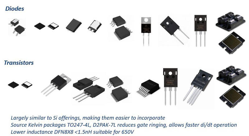
Figure 5: Typical range of package options available for SiC discrete diodes and transistors
Power ratings increase from left to right. Devices from 2A to 200A are available in separate formats. Source Kelvin packages are of interest in SiC transistors because they allow much faster switching.
Almost all Qorvo diodes and transistors use Ag sintering to attach the SiC die to the leadframe. It helps overcome thermal resistance challenges posed by chip thinning and shrinking chip size. In recent years, with the adoption of TO247-4L, D2PAK-7L, and DFN8x8 devices for SiC, this has happened in conventional packages such as D2PAK-3L, TO220-3L, and TO247-3L, which have large common source inductance. , to solve gate drive problems associated with high-speed switching.
Traditional 3-lead packages are the industry workhorse, but there is a move to "Kelvin source" packages because they offer cleaner, faster switching with little or no cost impact. Cascode devices have limitations in controlling turn-off transients by changing gate resistance, especially if delay times are desired to be long enough to prevent high-speed operation.
To manage it, Qorvo offers devices with discrete speed ranges that are internally pre-tuned for a specific maximum switching speed (UJ3C and UF3C series). If the circuit suffers from excessive voltage overshoot or power loop ringing, a small RC snubber is very effective with minimal loss effects. To assist the user, a user guide with gate drive and snubber recommendations to make the device easier to use is available on the Qorvo website.
Given the increased current density in SiC devices compared to silicon devices, packaging techniques have also improved to extract current from the source terminals on the top side of the chip. Techniques such as aluminum ribbon bonding, thick copper bonding wires using copper buffers, and bond-wireless packaging using Cu clips are among the main ways to extend the power cycle life of SiC transistors in both discrete and power modules. It's one.
The embedded package is also expected to enable further improved low-inductance architectures in the future, incorporating gate drivers and capacitors to minimize inductance while improving high-speed switching efficiency. A wide range of power modules are coming soon to the market, from small modules like Easy-1B/2B to large modules with the same footprint as standard IGBTs, such as 34mm, 62mm and EconoDUAL style modules.
For EV inverters, various technologies are optimized for SiC, from hybrid pack-style modules with pin-fin heat sinks to double-sided cooling options. Figure 6 shows an ultra-low inductance module proposed by Semikron that allows for very fast switching with manageable overshoot voltage. Figure 7 shows a SIP module from Apex Microtechnology incorporating a half-bridge driver and FETs and associated fast turn-on and turn-off waveforms using Qorvo 35mΩ, 1200V stacked cascodes.
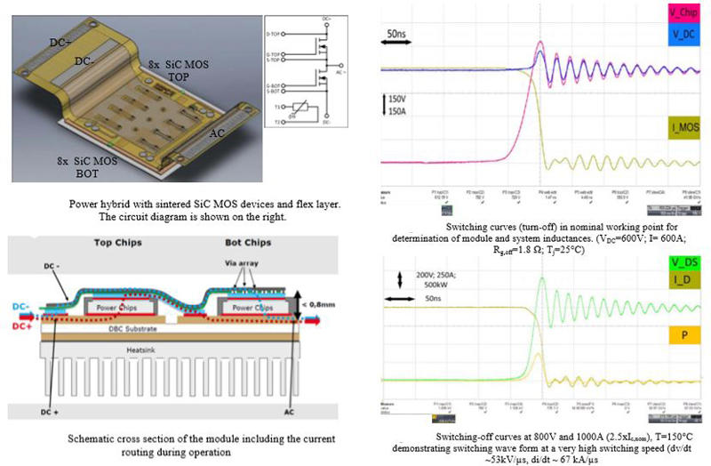
Figure 6: 400A, 1200V module with 1.4nH loop inductance demonstrated by Semikron in 2017
The reduced magnetic flux in a low-inductance design eliminates the fast-switching ON-state release of SiC, allowing for improved performance and lower system-level costs.
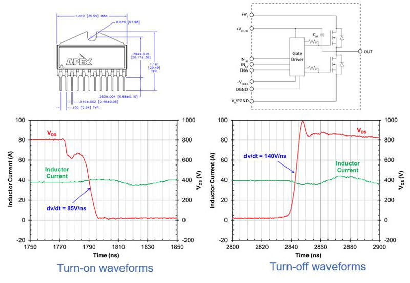
Figure 7: SIP module with Qorvo 35m, 1200V stacked cascode and embedded half-bridge driver
Used to switch at 40A, 800V with very fast rise and fall times. These advances simplify the use of high-speed devices, and the ability to use compact high-frequency designs to reduce passive components provides significant system-level cost benefits.
SiC devices have always been expected to offer significant advantages in higher voltage applications. The XHP type modules have been released initially with 3300V and 6500V modules, with 10KV coming soon. Qorvo offers a unique approach to this space using the Supercascode approach.
In this method, low resistance 1700V devices are connected in series to build a high voltage device, all controlled by a single low voltage FET at the bottom of the string. This approach is highly scalable and allows the implementation of modules from 3300V to 20KV without the need for high voltage chips. This is especially useful for implementing high-voltage solid-state circuit breakers and solid-state transformers that connect to medium-voltage grids.
Conclusion
Rapid advances in SiC device and package technology continue, increasing market acceptance for many fast-growing end-market applications. This will drive new WBG product development in many directions, from very fast switch devices for DC-DC conversion, EV on-board chargers and server power supplies to very low conduction loss modules for EV inverters. A number of next-generation system designs are underway that will take advantage of these improved WBG device capabilities, and the market will soon see a whole new level of power performance and efficiency brought about by SiC technology.
Inquiry
If you have any questions regarding this article, please contact us below.
Qorvo manufacturer information top page
If you want to return to Qorvo manufacturer information top page, please click below.
