
![]()
![]() Narrow down by specifying conditions
Narrow down by specifying conditions
現在1889件がヒットしています。check

Using Silicon Carbide (SiC) FETs in Data Center Power Supplies and Telecom Rectifiers
The introduction of 5G networks will lead to massive build-outs around the world, requiring many high-quality telecom rectifiers to supply the necessary power. There is renewed interest in WBG (Wide Bandgap) solutions to meet the need for increased efficiency, reduced operating costs, and reduced BOM costs. This is also common in efforts to make server power supplies more efficient than ever while minimizing heat loss. Powering the digital economy, big data, IoT and artificial intelligence, hyperscale data centers are now running over 30KW of server racks and highly sophisticated cooling management systems.
5G networks with larger antenna arrays (up to 64 transmit/64 receive) will deliver 100-1000 times higher data rates and will require even more power to serve the trillions of devices forming the IoT. will be needed. Many technological improvements have been made to reduce the power required for each base station, but many more are likely to be required. These base station power supplies must meet ever more stringent efficiency requirements from standby to full load conditions to accommodate advanced power management methods.
New SiC FETs are enabling previously unattainable efficiency goals, and this article examines the key topologies and device capabilities. Here's what we're seeing in this space where Si superjunctions, SiC FETs, and GaN FETs are all competing.
basic matters
Common to all of these power supplies is a power factor correcting PFC section that rectifies the output voltage of 400V from AC to DC with nearly unity power factor, and then this 400V to 48V for use in the system. Or has a DCDC converter that converts to 12V. Additionally, point-of-load converters are used to power the CPU and memory banks.
Examining the usage profile of data center server power supplies reveals that the majority of their operating life is at light to moderate loads. Therefore, the PFC and DC-DC sections must operate efficiently under all load conditions while meeting the thermal constraints of peak load operation. This can be captured by the well-known 80Plus standard used for computer power supplies, as shown in Figure 1. Servers must meet Titanium's requirements to maintain high efficiency even at 10% load. Figure 2 shows a typical specification taken from the Open Compute Project, featuring Titanium+ requirements for a 3.3KW class power supply.
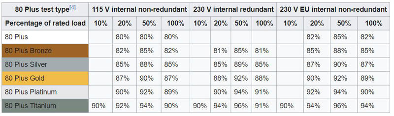
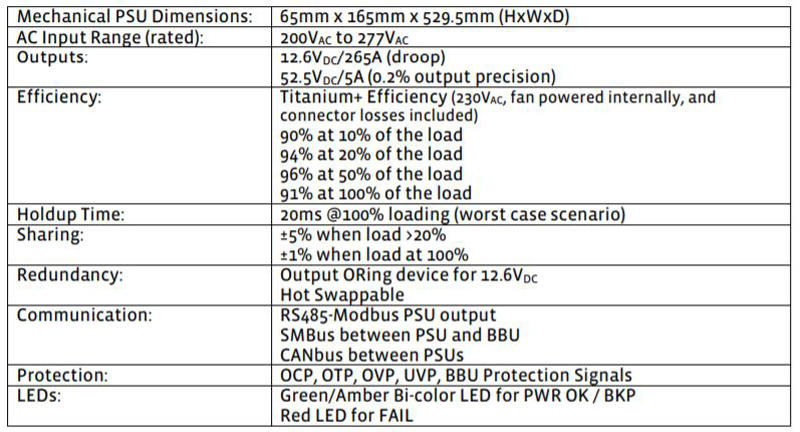
Figure 3 features an input bridge rectifier, a simple dual interleaved boost converter (PFC) with 650V FETs and SiC JBS (junction barrier Schottky) diodes, and a full-bridge LLC stage for a DC-DC converter. shows a typical power supply architecture. Input EMI filter is not shown. A typical switching frequency of 65-150 kHz is used for the PFC stage. The need for power density is traded off for high efficiency at low frequencies because here the inductor can be made to peak current instead of 30kHz. For this reason, Si superjunction MOSFETs with SiC JBS diodes are used to maintain high efficiency while performing high-speed switching between 65kHz and 150kHz. Highly advanced superjunction MOSFETs can switch fast and SiC Schottky diodes can minimize MOSFET turn-on losses.
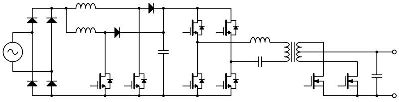
After the input bridge rectifier there is an interleaved PFC stage and a full bridge LLC stage.
A 650V MOSFET is also commonly used for the LLC portion of the circuit. This circuit maintains ZVS (Zero Voltage Switch) operation and reduces turn-off current, resulting in significantly lower losses, enabling operation at high frequencies from 100 to 500kHz, and miniaturizing the transformer. I can. On the secondary side, a very low on-resistance 80-150V silicon MOSFET is used to rectify the high frequency secondary AC voltage and provide a DC voltage output. The 650V FETs used are chosen so that body diode recovery is not destructive even in the absence of ZVS under some operating conditions.
semiconductor device
Mainly transistors, 650V class devices are generally used on the high voltage side of PFC and DC-DC units. Table 1 provides an overview of current silicon, GaN, and SiC devices and their relevant properties. In terms of RdsA converted to chip size, SiC FET (SiC JFET RdsA) is the best choice. All wide bandgap devices have better body diode recovery characteristics compared to silicon superjunctions. However, only SiC and silicon devices can handle avalanche energy. Enhancement-mode GaN devices have low Vth, coupled with speed and narrow gate voltage range, making them difficult to drive.
|
Spec |
SIC Cascode UJCO6SOSK |
SiC MOSFET |
E-mode GaN |
Si Superjunction |
|
Rpm mohm-cm2 |
0.75 |
3.5 |
6.6 |
10" |
|
Rds*Eoss mohm-uJ |
255 |
600 |
350 |
462 |
|
Vth (V) |
5 |
4.5 |
1.3 |
3.5 |
|
Avalanche |
Yes |
Yes |
No |
Yes |
|
Gate voltage rating (V) |
±25 |
±22/-4 |
+/-10 |
+/-20 |
|
Diode behavior |
Excellent |
Excellent |
Excellent |
Poor |
Table 1: Basic Technology Comparison of 650V Transistor Options
Table 2 shows a comparison of some industry equivalents in commonly used TO-247 packages. Silicon superjunction (Si SJ) devices and UnitedSiC can be driven with 0-10V drive. SiC MOS options require different voltages (eg -4V to 18V). All SiC devices offer lower input capacitance (gate charge) and significantly reduced diode recovery charge Qrr. Silicon superjunction and SiC FETs have lower body diode conduction losses than SiC MOSFETs.
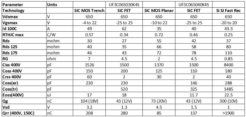
Table 3 shows a comparison of similar devices with a DFN8x8 footprint. Silicon SJs, SiC FETs, and GaN devices can all be driven with standard silicon gate drives. UnitedSiC FETs offer very low on-resistance. A comparison of the R DS(ON) at 150°C for each device is best done using the figures of merit in the bottom three rows. The WBG solution offers better figures of merit, especially for Rds*Coss(tr) and Rds*Qrr.
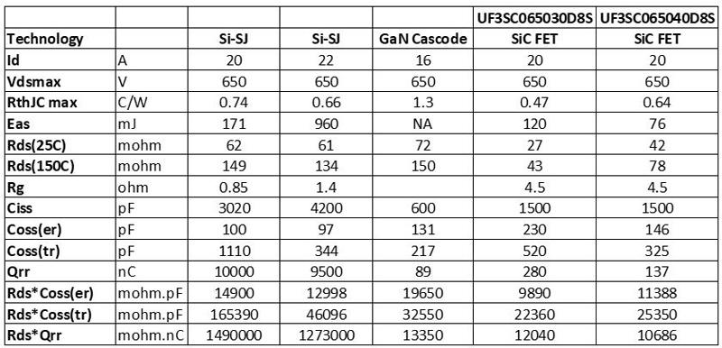
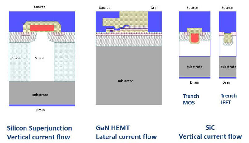
Figure 4 shows the cross-sectional architecture of commonly used configurations of SiC, GaN and silicon superjunction FETs. GaN HEMTs are horizontal devices, while others are vertical current devices. Vertical current flow allows for more compact packaging of high voltage devices because the source and drain terminals are on opposite sides of the wafer rather than on the top side of the wafer. In GaN HEMTs, conduction is limited to 2DEG channels, whereas SiC devices use short surface channels, mostly as bulk to carry current. The SiC JFET has a bulk channel and along with its verticality, it has the lowest resistance per unit area (RdsA), enabling a small chip size. It is then cascoded with a low voltage Si MOSFET (increase the resistance by 10%) to form a SiC FET.
As the device improves, the load current charging the device's output capacitance Coss will eventually set the switching speed limit. A low value of Coss(tr) for a given on-resistance gives the fastest slew rate and shortest delay time to reach 400V. As can be seen from Table 3, SiC FETs excel in this regard and are suitable for high frequency power conversion.
Regarding Qrr, all of the WBG options offer much better performance than silicon superjunction devices. Therefore, these devices are chosen whenever the circuit uses a hard switch turn-on, such as a CCM (continuous current mode) totem-pole PFC. If these circuits use body diode conduction in the freewheeling state, the voltage drop due to the on-state will lead to conduction losses. Synchronous conduction is therefore commonly used with the FET channel turned on to reduce these losses. There is typically a delay between detecting current reversal and turning on the FET channel, which at high frequencies is a significant fraction of the switching period. For example, if the switching frequency is 100kHz (10us period), the 100ns dead time for diode conduction is of little concern. However, it becomes 10% for a switching cycle of 1MHz (1000ns period). Therefore, low Qrr and low body diode conduction losses VSD are useful properties, and Qorvo's SiC FETs offer both.
Regarding device robustness, all SiC devices have excellent avalanche capability, which enhances system reliability of the converter. Despite the small chip size, it often exceeds the capabilities of superjunction FETs, especially at high current levels. GaN devices cannot handle avalanche, so they are designed with high voltage to avoid this region of operation. Figure 5 shows a scope capture of a 40mΩ, 650V SiC FET from UnitedSiC handling a peak avalanche current of 80A (blue), which far exceeds practical needs. You can see that the breakdown voltage is over 800V (green).
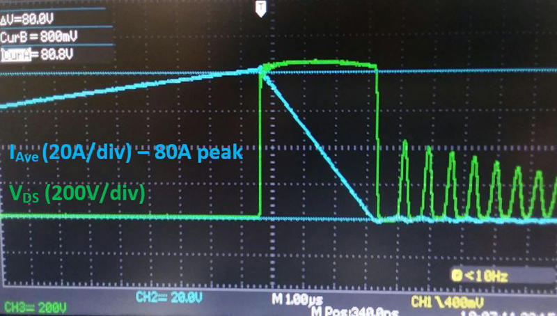
Despite the SiC JFET's small size, the device handles avalanche currents of over 80A without failure.
Gate drive considerations
Using SiC FETs simplifies the gate drive because the low-voltage MOSFETs have a VTH threshold of 5V and a VGS(MAX) rating of +/- 25V. It can be driven like a 0-10V (or 12V) silicon superjunction MOSFET. Figure 6 compares recommended gate drive voltages and corresponding gate absolute maximum ratings for various technologies. SiC MOSFETs typically require negative and positive gate drive, with a total gate voltage swing of 20-25V. Gate voltages are often very close to the absolute maximum ratings, so gate spikes need to be taken care of. Large gate voltage swings can result in significant gate charge loss at high frequencies. Additionally, manufacturers' recommendations for gate drive voltage levels must be carefully followed to manage VTH hysteresis issues. SiC FETs are flexible in this regard and do not require such careful control of gate voltage levels, but they can also be driven with gate voltages compatible with SiC MOSFETs.
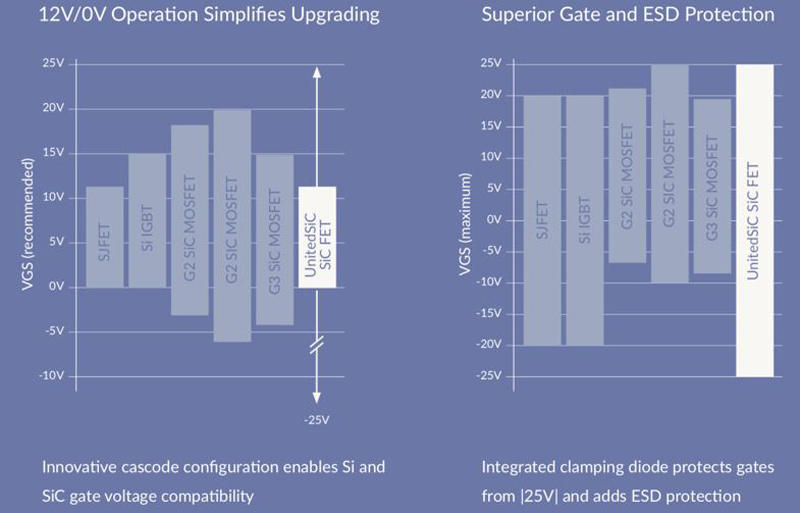
SiC FETs are uniquely versatile.
GaN enhancement-mode devices typically have a lower Vth and a narrower gate voltage range, so they are often very close to the absolute maximum VGS limit. This requires special drivers and careful layout to avoid damage to the switches. Cascode options can get around some of these problems. The smaller gate voltage swing of enhancement-mode devices helps reduce gate losses at high frequencies.
In all cases, as devices are used at higher speeds, it becomes increasingly difficult to maintain them at high dV/dt. The same is true for managing gate voltage spikes from the power loop and gate drive loop inductance. Deploying a package with a source Kelvin pin helped, but I'll discuss other options later in this article.
Circuit Topology – PFC Stage
Figure 7 shows the efficiency measured at 100kHz on a 1.5KW Qorvo demo board using a totem-pole PFC (TPPFC) circuit and a UJC06505K SiC FET. This circuit eliminates the conduction losses of a PFC composed of an input diode bridge and SiC. In this case the converter works in CCM mode and the device is hard-switched.
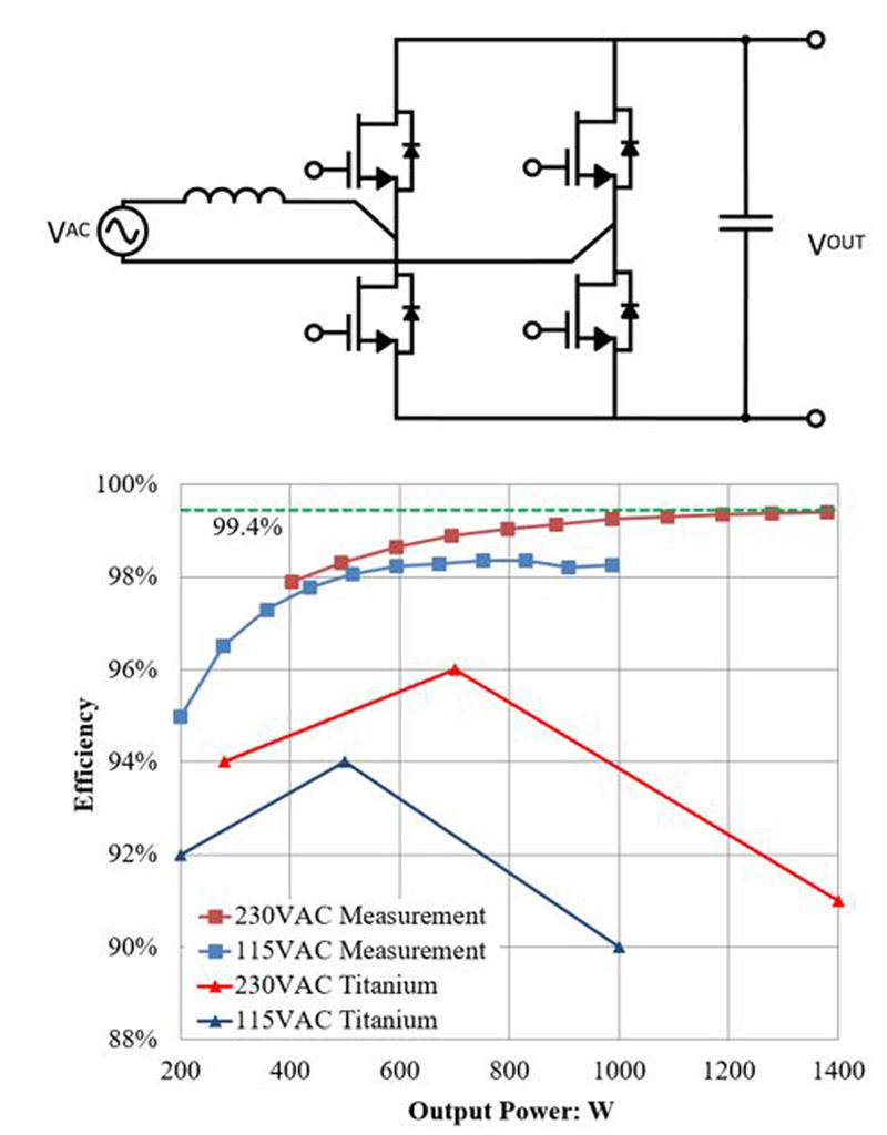
Figure 8 shows an interleaved TPPFC that can be designed using coupled inductors. This circuit can be used in continuous current mode. Alternatively, it can operate at much higher frequencies in critical conduction mode because it eliminates turn-on losses. SiC FETs allow very high power densities without sacrificing efficiency, but add control and magnetic design complexity when ripple currents are high and the current zero crossing needs to be detected. .
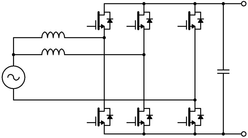
It employs two fast switching and one line frequency switching half-bridge. The coupled-inductor approach allows the use of critical conduction mode operation, which allows for significant frequency increases.
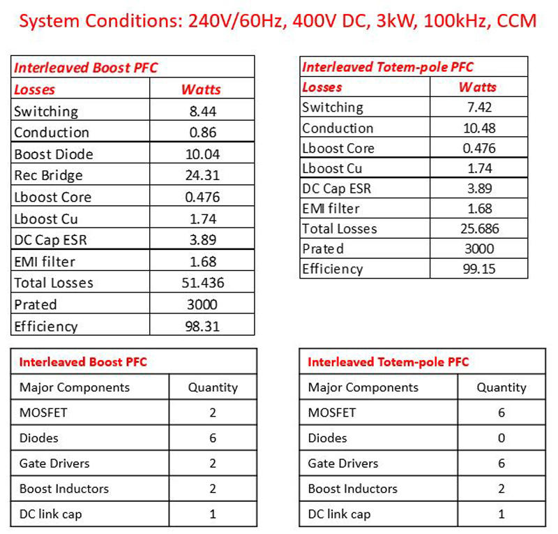
Table 4 shows a comparison of the loss breakdown using the interleaved PFC topology shown in Fig. 1 and the interleaved totem-pole PFC in Fig. 8. In both cases, we are assuming a 3KW class converter with each switch running at 100kHz. Interleaving means that the inductor ripple frequency appears to be 200kHz. The Totem Pole PFC significantly reduces losses (25.7W vs. 51.4W), allowing Titanium to meet its net efficiency goals. This is pushed forward by eliminating the 24.3W loss from the bridge rectifier. The totem-pole PFC used in this example requires four more FETs and a gate drive circuit.
Another method that does not require current crossing detection is to use an additional auxiliary switch to achieve zero voltage transition at turn-on. Similar or better results can be obtained using resonant techniques such as Auxiliary Resonant Commutating Pole (ARCP), which eliminates both turn-on and turn-off losses. However, the price-performance with more advanced technology only seems to benefit at power levels well above 5KW.
Circuit Topology – DC-DC Stage
With a fixed output voltage, the full-bridge LLC converter in Figure 1 offers excellent power density and efficiency and is now an industry workhorse at higher power levels. At lower power levels, a half-bridge LLC implementation can be used. Frequencies in the 100-500kHz range are commonly used for high current applications at 12V output, and the main loss reduction efforts are to improve the transformer on the secondary side and the MOSFETs on the secondary side. Become the Lord.
For high voltage FETs, the VDS transition from off state to diode conduction requires charging the output capacitance. A low COSS(TR) is required to do this quickly. However, the dead time should be minimized before driving the FET to reduce losses due to body diode conduction. The low on-state resistance minimizes conduction losses, and the low EOFF of most superjunction and WBG switches minimizes switching losses.
Prospects for the near future
Improvements in silicon superjunction FETs continue, but the level of improvement in SiC and GaN devices over the next few years will far exceed what can be achieved with silicon. In addition to improving RdsA (30-50% improvement every 2-3 years), we expect many improvements in packaging technology. The main challenges are lower inductance and more efficient heat removal in small surface mount packages.
One possible approach is to move to half-bridge elements designed either directly surface-mounted or embedded in the PCB. This simplifies the PCB layout, lowers inductance, and allows for improved gate loop circuits.
Another option is to integrate the driver and power device, i.e. as a single driver + switch or half-bridge element. Since most SiC and GaN devices require unique drive voltage levels and circuitry, this complexity is absorbed in packaged, integrated products, making it easier for users. Plus, you can get the most out of each device. This will undoubtedly lead to significant savings in system cost and power dissipation, facilitating the adoption of WBG.
As mentioned above, a SIP half-bridge with integrated half-bridge gate drive using 35m, 1200V SiC FETs was discussed in a previous article in this series. Surface mount options are emerging from various suppliers and the trend will accelerate.
The cost of 650V-WBG switches is dropping rapidly. The Qorvo 650V FET is expected to approach price parity with silicon within the next two years. In this regard as well, in addition to ease of use, it is expected to rapidly accelerate the deployment of WBG devices in server and telecom power applications.
Inquiry
If you have any questions regarding this article, please contact us below.
Qorvo manufacturer information top page
If you want to return to Qorvo manufacturer information top page, please click below.
