
![]()
![]() Narrow down by specifying conditions
Narrow down by specifying conditions
現在1888件がヒットしています。check

This article examines the benefits of applying SiC technology in EV traction inverters. It shows how the efficiency of the inverter improves under all load conditions, from light load to full load. Using a higher operating voltage with a highly efficient 1200V SiC FET helps reduce copper losses.
You can also increase the switching frequency of the inverter to output a more ideal sinusoidal waveform to the motor windings and reduce iron losses in the motor. All of these factors are estimated to improve battery electric vehicle (BEV) performance by 5-10%, and reducing losses can alleviate cooling problems.
Consideration of adoption of SiC in automotive applications
Recent news is that battery electric vehicles are clearly moving faster than previously thought. This is the result of a renewed effort by automakers (both incumbents and start-ups) to create the best technology to get the most out of expensive battery packs and improve their performance. Maximizing efficiency and reducing size and weight has become a reality.
As a result, SiC transistors have rapidly penetrated into EV on-board chargers and DC-DC converters. Given that traction inverters must handle ten times the normal power levels, SiC transistors could change the landscape of power semiconductors used in traction inverters. To do so, SiC technology must clear all the necessary hurdles to provide clear cost-performance advantages and enable reliable and manufacturable inverter system designs.
The boost stage used before the inverter can definitely use SiC for the same reasons as previously described for on-board chargers and DC-DC converters. This article describes the main advantages of SiC technology for EV inverters and describes some implementation schemes based on Qorvo's technology.
Main advantages of SiC technology
The drive cycle of a typical EV, especially one used in an urban environment, uses the inverter in the light to medium load range during its operating life, with frequent stops and starts. But inverters must be designed to withstand all the worst stresses, such as hard acceleration, steep climbs, and operation over a wide range of ambient temperature conditions.
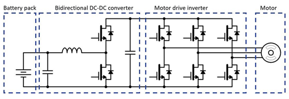
Figure 1 shows a typical two-level voltage source inverter that can be used to drive an internal permanent magnet motor. This is the configuration commonly used in BEVs, where the inverter is placed close to the motor. Inverter switches are usually controlled such that a three-phase AC voltage is applied to the motor windings.
This is done by turning the power switch on and off as instructed by the controller at frequencies between 4 and 10 kHz to produce a fundamental AC frequency of up to 1 kHz. Typical vehicle EV total power levels range from 50 to 250 kW. The DC voltage used depends on the battery system, and a boost converter is used to output a fixed voltage for the inverter even if the battery voltage varies.
This voltage is currently 300-500V, but could reach 600-800V in the near future. For the same power, you can get a lower current by supplying a higher voltage. As a result, copper loss can be reduced.
Power switch losses come in the form of conduction losses that occur when the switch is carrying current, and switching losses that occur when the switch is turned on or off. Conduction losses are independent of switching frequency, whereas switching losses are directly proportional to the frequency used.
Figure 2 shows the characteristics of SiC FETs and silicon IGBTs. At any current, conduction losses are given by the ID * VDS product. Therefore, unipolar SiC FETs benefit at all current levels up to 200A due to the lack of knee voltage seen in IGBTs. It is especially beneficial at low currents for light and medium load operation.
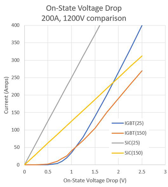
Figure 3 is a graph comparing the conduction and switching losses between low conduction loss IGBTs and SiC FETs in a 750 V inverter operating at 8 kHz on a 400 V bus. IGBT-based solutions have significant switching losses even at 8kHz, so they cannot be used efficiently at 25kHz. The SiC-based solution not only has low conduction losses at all output levels, significantly reduced losses at 8 kHz, but can also be used at higher inverter frequencies with higher efficiency.
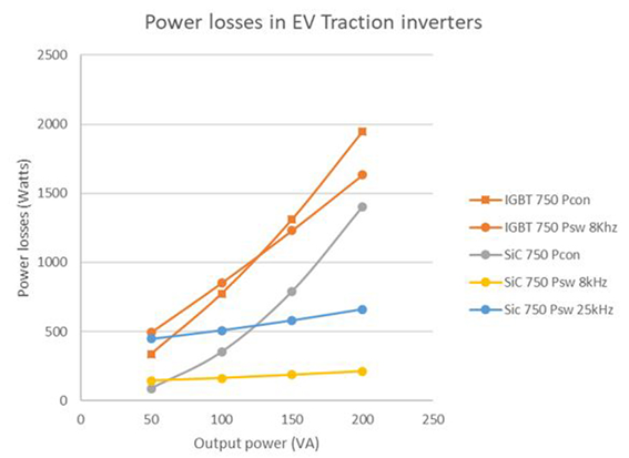
Loss differences are seen for all conditions, but are very large at 25kHz
Another aspect of EV inverters is that they require bi-directional power transfer, unlike traditional industrial motor drives. During regenerative braking, a switch is controlled so that the same inverter acts as a rectifier and the motor acts as a generator, allowing power to be returned to the battery.
SiC FETが第3象限損失においても同程度の低導通損失が可能であるという事実は、同期整流を使用して、この動作モードでも損失を非常に低く保つことができることを意味します。これはIGBTでは不可能であり、逆並列フリーホイールダイオードは、より高い損失で逆潮流を処理します。
Rated voltage
Many EV inverters today use 750V IGBT solutions to operate inverters with bus voltages in the range of 300-500V. Battery voltages of 600-800V can be used with a 1200V switch to handle high power more efficiently.
Table 1 compares some features of a 450A, 750V half-bridge module used in a 200KW BEV traction drive based on low conduction loss IGBTs and a 750V rated UnitedSiC FET. Three IGBTs and three diodes are used for each switch position. These are replaced by six stacked SiC FETs with a resistance of 5.4mohm and less than half the size.
Cases 1 and 2 in Table 1 show the difference in total conduction, switching and total total losses at 8kHz. The total losses are halved at 200kW and nearly a quarter at 50KW. SiC FETs are very effective because most of the time the inverter operates at light loads. Note that both conduction and switching losses are lower in SiC FETs. But the switching loss difference is almost 8 times less than SiC FET at 200KW.
It is also shown that the same module can be used up to 300KW while keeping all FETs below Tj = 150C. This means you can use the same inverter hardware for your 300KW system. Now look at Case 3 in Table 1. Even better, 300KW with 8 SiC FETs per switch can reduce the peak loss when using the module from 3425W to 2666W.
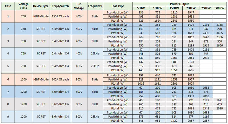
The bottom half compares a 400A, 1200V IGBT module with a 1200V SiC FET module used in a 200kW inverter. In all cases, a fin heatsink type 3-phase module was installed and the coolant temperature was 90°C. Even if the SiC FET is rated at 175C and can be used at 200C for a short period of time, the maximum junction temperature is kept below 150C in all cases. Using low switching losses when running the inverter at 25kHz can improve waveform quality and reduce iron losses in the motor. Even in this condition, the SiC FET solution (Case 4 in Table 1) shows lower losses than the IGBT solution under all load conditions. At 200KW output, the IGBT solution consumes 3580W at 8kHz while the SiC FET solution consumes only 2061W at 25kHz. This module can output 250KW with 6x parallel SiC FETs.
スイッチごとに4X SiC FETを使用するだけで、低損失になり低コストが実現できます。これは表1のCase5に示されており、損失はIGBTベースのソリューションの損失を大きく下回っています。
The bottom part of the table compares the losses when 1200V transistors are used and the operating bus voltage is 800V. 4 IGBTs and 4 diodes per switch (Case6), 4 SiC FETs per switch (Case7,9). Losses at 8kHz with SiC FETs are less than half at full power and a quarter at 50KW output. Case8 shows that the same module can be easily scaled up to 300KW operation using 6X SiC FETs per switch.
Switching these IGBTs at 25 kHz is not possible due to excessive switching losses, but Case 9 shows how this can be achieved with SiC FETs while maintaining high efficiency. Losses are well below those of an IGBT operating at 8kHz. Smooth waveforms also help keep motor iron losses low, and inverters switch at frequencies well beyond the audible range. Note that in all cases the modules provide higher power output with the same footprint.
extreme conditions
An important safety requirement for all motor drives, including EV inverters, is their ability to withstand short circuits that may occur during maintenance or operation. Such shorts can occur between DC buses, from a motor winding to ground, or between windings. For a solid-state switch, this means that the switch may have to withstand a short-circuit condition when the switch turns on until the gate drive circuit detects the condition and turns the switch off within 3-5 µs. To do.
Alternatively, a short circuit may occur when the switch is already conducting. In any case, the switch must be able to withstand these events. Regardless of the chip's starting temperature when such an event occurs, the characteristics of the device must not change in such a way as to shorten the life of the device.
Figure 4 compares the difference in short circuit withstand (SCWT) of IGBTs, SiC MOSFETs and SiC FETs. SiC MOSFETs have very high peak currents during short circuits that can damage the MOSFET gate oxide. This can be managed by using a low gate voltage drive. This reduces short-circuit current, but significantly increases conduction losses.
SiC FETs, which consist of Si MOSFETs stacked on SiC JFETs, are much better at this. With minimal change in conduction loss, peak saturation current can be adjusted to provide the required short-circuit withstand capability. This saturation current is set by the JFET and is independent of the VGS applied to the MOSFET. Experiments have shown that this type of stress can be safely handled by SiC FETs for over 100 repeated events. Moreover, the device handles such short circuits even with a starting chip temperature of 200°C.
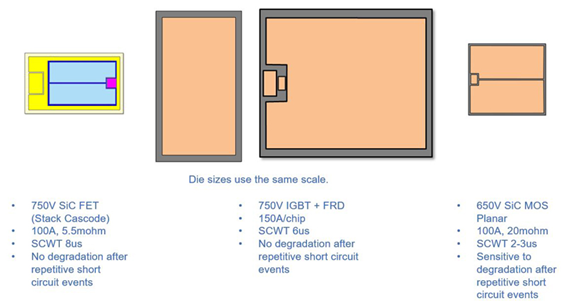
The semiconductors in Figure 4 are drawn to scale and the SiC FET is the smallest chip size 100A device. The ability to withstand the extreme heat generated during a short circuit is a key advantage of SiC JFETs on which SiC FET stack cascodes are based. The difference in chip size means that SiC FETs can be used to significantly reduce the on-resistance for a given module footprint.
A technological approach to SiC-based inverters
The most common topology for inverters is the venerable two-level voltage source converter in Figure 1. The type of switching used in such inverters is called hard switching, which results in significant overlap of high voltage and current through the switches during the transition.
Based on the results in Figure 3, one approach designers can take is to use fast-switching SiC devices to reduce both switching and conduction losses, even at frequencies up to 25kHz. In that case, switch transitions occur at high dV/dts. With BEVs, long cable lengths between the inverter and the motor are not a problem as in standard industrial drives. However, high dV/dt waveforms applied directly to the motor windings can induce large displacement currents in the insulator.
This can be rectified using a filter at the inverter output, a so-called dV/dt filter or a high dV Smooth only the /dt part. The higher the switching frequency, the easier the filtering. Reducing ripple in the current waveform is predicted to improve overall motor efficiency by 1-3% and extend motor life. This efficiency advantage contributes to an extended voltage range or reduced battery size.
Another approach is to keep the switching at a low frequency of 5-8kHz and operate the device at very slow dV/dt rates (e.g. 8V/ns or less). In that case the cycle-by-cycle switching losses can be higher, but the lower frequency allows the total total power loss to be managed.
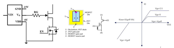
Figure 5 shows the recommended technique for using SiC FETs in this situation. A stacked low-voltage MOSFET is used as an enable switch to ensure normally-off operation during start-up and short-circuit fault conditions, while the SiC JFET gate is turned on/off directly. This allows very low dV/dts with optimal losses. This scheme allows excellent short-circuit handling capability and can further reduce conduction losses by 15-20% if the JFET gate is driven to +2.5V instead of 0V.
To manage 3rd quadrant conduction, a JFET can be used with a short dead time, or a small JBS diode can be added to allow freewheeling current only during the dead time. The graph on the right side of Figure 5 shows the operation of the SiC JFET in the third quadrant.
This makes it easier to implement low dV/dt switching
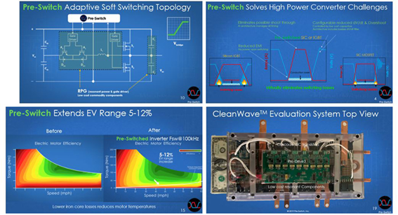
A more complex approach, but one that can achieve the highest efficiency, is to apply fully resonant switching, as in the newly developed controller by Pre-Switch Inc, as well as the auxiliary resonant commutation pole method. Figure 6 shows typical switching waveforms that completely eliminate turn-on and turn-off switching losses while maintaining circuit topology and low dV/dts. Although this circuit helps reduce IGBT switching losses and improve efficiency, IGBTs still suffer losses due to the need to remove the stored charge each cycle.
Furthermore, the effect of knee voltage on conduction loss on the IV curve remains. Therefore, peak efficiency under all load conditions is best achieved by SiC FETs, which are unipolar devices with no tail current and knee voltage. The converter can also operate at very high frequencies of 50-100kHz, resulting in a smoother sine wave output. This can reduce iron losses and further increase motor efficiency. This, coupled with minimal power loss in the inverter, can extend the maximum power range of the BEV. An example of a compact 200kW inverter using this method with SiC FETs is shown in Figure 6.
Conclusion
This allows SiC FETs to achieve very high power densities without high dV/dt switching issues. The result is improved motor operating efficiency and inverter efficiency.
Detailed investigations by many industrial and academic groups have concluded that SiC MOSFETs offer distinct advantages for improving the efficiency of traction inverters and extending the range of BEVs. This article explained the rationale for this evaluation and examined the robustness needs of power transistors used in SiC inverters.
We considered three implementation topologies for BEV inverters that allow the user to choose the method that best suits the constraints of the overall system. For the highest efficiency, the ARCP scheme eliminates all switching losses, allowing you to take full advantage of the ultra-low conduction losses offered by SiC FETs.
Inquiry
If you have any questions regarding this article, please contact us below.
Qorvo manufacturer information top page
If you want to return to Qorvo manufacturer information top page, please click below.
