- Semiconductor BusinessHOME
- Products and Services of Macnica,Inc.
-
technical information

-
Events and Seminars
- Handling Manufacturer
- Support
- Inquiry
- Click here to purchase products
- Semiconductor business e-mail magazine registration
![]()
![]() Narrow down by specifying conditions
Narrow down by specifying conditions
現在2182件がヒットしています。check

The printed circuit board (PCB) that houses the Ethernet PHY is one of the most EMI, ESD and other factors affecting overall performance. In this column, I would like to introduce some key points related to board design for Ethernet PHY peripheral circuits.
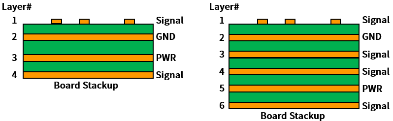
PCB Layer (Stackup)
A PCB with at least four layers is recommended to implement the Ethernet PHY and design a PCB that meets the signal quality and performance requirements. Figure 1 is an example of a 4-layer and 6-layer PCB Stackup.
Ethernet Layout Example
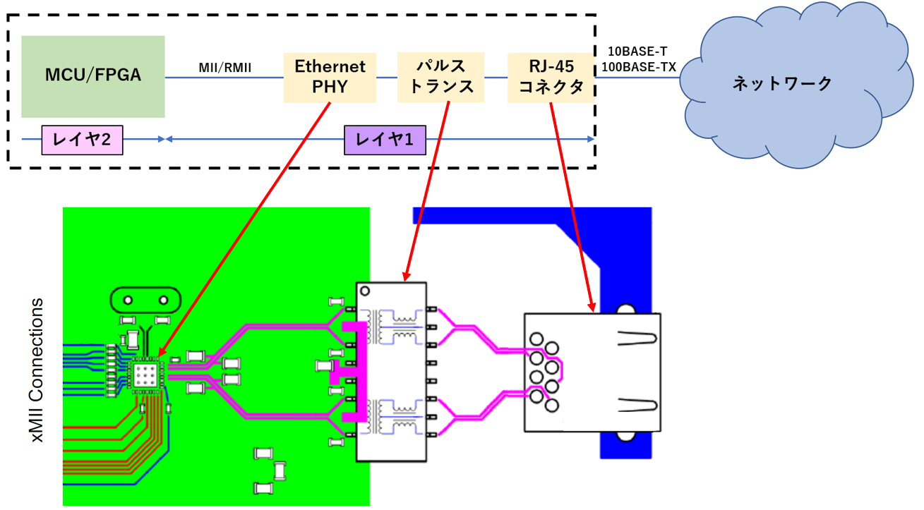
Figure 2 shows the H/W configuration of a typical Ethernet interface. Layer2 consists of MCU and FPGA, and Layer1 consists of Ethernet PHY, pulse transformer and RJ45 connector.
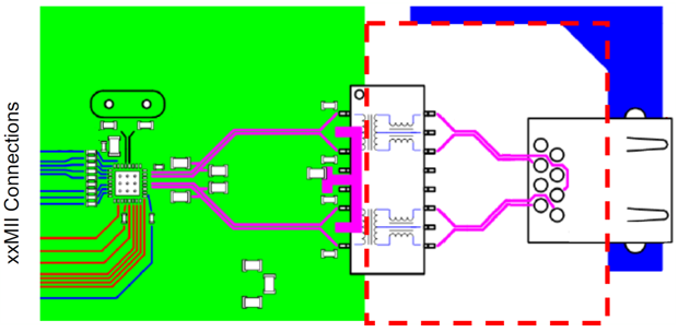
Transformer Area
Figure 3 shows the Transformer Area (the area surrounded by the red dashed line). Note the following points in the transformer area PCB design:
・Avoid arranging the power and ground planes of all board layers under the transformer.
・Extend the chassis ground to the RJ45 beyond the transformer.
・Do not wire digital signals between the PHY and the RJ45 connector.
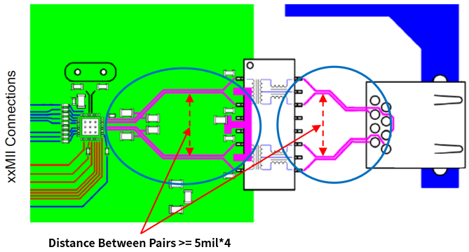
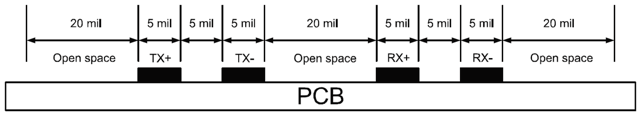
Differential signal layout
Figures 4 and 5 are examples of differential signal layout and transmit/receive differential pair signal placement.
Differential signal layout is very important from the point of view of signal quality and performance. Note the following regarding the layout of differential signals:
・Differential pairs (TX+/- or RX+/-) should be separated from other signals and routed with 5mil traces with 5mil trace spacing,
Control the impedance to 100Ω with equal length wiring.
・Differential pair traces should be as short and symmetrical as possible.
・Differential pairs should be placed and routed on the same board layer.
• Stubs should be avoided on all signal traces, especially on differential signal pairs.
• Differential pairs should be separated from each other by at least four times the 5 mil trace spacing.
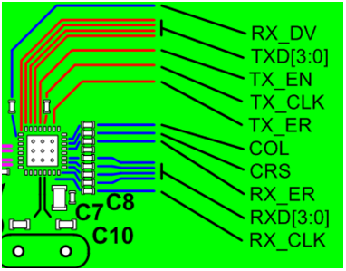
MAC Interface (MII/RMII)
There are also some notes on the layout of the MAC Interface that connects the PHY and the MAC.
・Each signal of MII and RMII is controlled to 68Ω impedance.
• The transmitted signal group and the received signal group are each traced together. (See Figure 6)
・MII and RMII signals should be traced as short as possible.
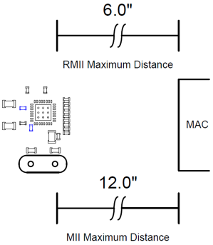
Recommended maximum trace length is 12 inches or less for MII and 6 inches or less for RMII. (See Figure 7)
・When bending the wiring, avoid bending it at 90 degrees, and bend it at 45 degrees.
Summary
The above are the basic points to note when designing the PCB for the Ethernet PHY peripheral circuit.
When designing, we recommend that you check the Application Notes and H/W Design Checklist issued by the IC Vendor.
Microchip Ethernet related product information
Click below for information on Microchip's Ethernet related products.
Inquiry
If you have any questions regarding this article, please contact us below.
To Microchip manufacturer information Top
If you want to return to Microchip manufacturer information top page, please click below.