- Semiconductor BusinessHOME
- Products and Services of Macnica,Inc.
-
technical information

-
Events and Seminars
- Handling Manufacturer
- Support
- Inquiry
- Click here to purchase products
- Semiconductor business e-mail magazine registration
![]()
![]() Narrow down by specifying conditions
Narrow down by specifying conditions
現在2189件がヒットしています。check

I would like to introduce [soft error (SEU) resistance], which is a feature of Microchip 's non-volatile FPGA, in three parts.
In Part 2, I will explain the soft error (SEU) resistance due to [differences between FlashROM and Flash-based FPGA].
Features of Flash ROM
FlashROM is widely used as a general-purpose storage and has become common. Flash ROM stores data in the Flash cells themselves. This section briefly summarizes the FlashROM method and structure.
Floating gate method / charge trap method
- The floating method retains data by charging a PolySi (polysilicon) film sandwiched between SiO2 (silicon dioxide) layers.
- The charge trap method replaces the floating PolySi with SiN (silicon nitride) and stores charge in SiN charge trap cells.
SLC, MLC, TLC, QLC
- SLC (Single Level Cell) has 1 bit per cell and 2 values with Hi or Low.
- MLC (Multi Level Cell / MLC-2) represents 4 values from 11 to 00 with 2 bits per cell.
- TLC (Triple Level Cell / MLC-3) represents 8 values from 111 to 000 with 3 bits per cell.
- QLC (Quad Level Cell / MLC-4) represents 16 values from 1111 to 0000 with 4 bits per cell.
NOR type / NAND type
In the NOR type, all cells are connected to bit lines and source lines. Generally called serial flash, it is often used in applications that require high reliability. However, with the miniaturization of semiconductor processes, soft errors have reached a level that cannot be ignored, so it is now said that ECC (error correction) must be used even in NOR-type Flash. Compared to the NAND type, read is faster, but it is not suitable for large capacity and write is slow.
In the NAND type, cells for the number of pages are connected in series. In general, it is often used as a storage device for mobile devices such as USB memory, SSD, and mobile phones. Compared to the NOR type, it is said to have a large capacity and low cost.
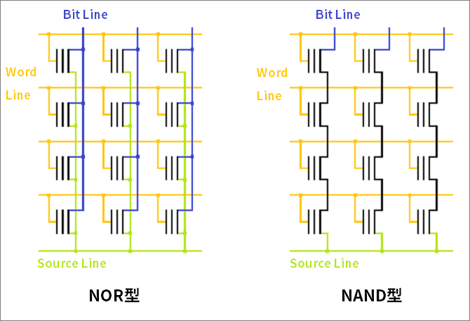
Figure 1 NOR type and NAND type
Features of FlashFPGA
Here we introduce the structure of the Flash-based FPGA.
Flash cells in FPGAs, unlike Flash cells in general flash memory, act as switches in the wiring structure. Figure 2 shows a representative example of a Microchip FPGA Flash cell structure. Structurally, it has a so-called 2T type Flash structure, sharing a floating gate and having a physical size. The Flash cell on the “Sense” side plays the role of programming (writing). On the other hand, the Flash cell on the “Switch” side plays the role of logic operation (wiring switch).
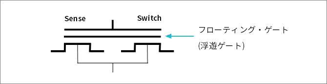
Figure 2 Flash-based FPGA cell structure
Next, I will explain the relationship between Flash cells in Flash-based FPGAs and logic cells in FPGAs. As shown in Figure 3, Microchip's Flash-based FPGA differs from other companies' SRAM-based FPGAs in that the intersection of the wiring structure is directly a Flash cell.
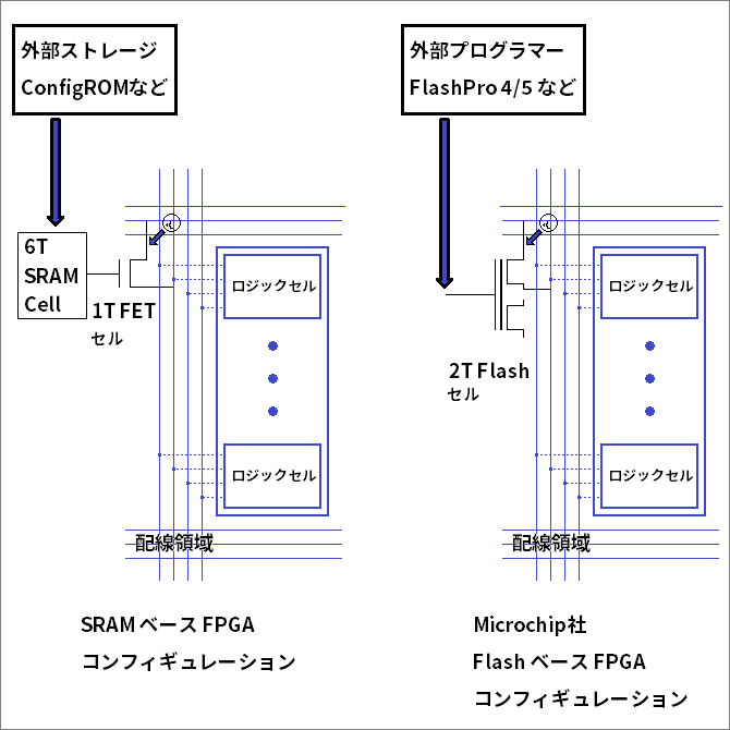
Figure 3 FPGA structure
Difference between FlashROM and Flash-based FPGA
So far, we have explained the structure and method of FlashROM and Flash-based FPGA, but I would like to sort out the differences between FlashROM and Flash-based FPGA. A brief summary of the differences between
- Structural difference: Structure is different from NOR type and NAND type FlashROM.
- Differences in method: Flash-based FPGAs have their own built-in features, such as a large amount of charge that is charged by adopting 2T Flash cells, for example.
From these differences, you can see that Flash-based FPGAs have high SEU resistance.
SEU resistance
So far, we have explained the structures and methods of FlashROM and Flash-based FPGAs. Microchip FPGAs are highly resistant to SEU. On the other hand, it can be said that SRAM-based FPGA has a structure that is susceptible to SEU. The NOR type of FlashROM was said to be highly resistant to SEU due to the old process technology, but in the process of advanced miniaturization, SEU is in a region where SEU cannot be ignored, and countermeasures such as installing ECC are taken to maintain SEU resistance. . In the NAND type, it is generally considered to be premised on the premise of incorporating ECC and software countermeasures on the premise that soft errors will occur.
|
technology |
SEU |
|
Flash-based FPGAs |
Not detected |
|
SRAM-based FPGAs |
detection |
|
NAND (MLC) |
vulnerable |
|
NAND (SLC) |
Not detected |
|
NOR |
Not detected |
Table 1 SEU resistance
Summary
Did you understand the difference between FlashROM and Flash-based FPGA?
A brief summary of the differences between
- Structural difference
- difference in method
From these differences, you can see that Flash-based FPGAs have high SEU resistance.
That was the [Difference between FlashROM and Flash-based FPGA].
Inquiry
If you have any questions regarding this article, please contact us below.
To Microchip manufacturer information Top
If you want to return to Microchip manufacturer information top page, please click below.