
![]()
![]() Narrow down by specifying conditions
Narrow down by specifying conditions
現在1888件がヒットしています。check

In the design and development of "in-vehicle products", there are increasing cases where "FPGA" works more effectively than conventional ICs such as SoC and CPU.
In a previous article, I introduced how the features of FPGA can be utilized in the trend of automotive products.
In particular, there are many situations where it can demonstrate its merits in in-vehicle products that require “image processing”.
Manufacturers dealing with in-vehicle products are also expected to have FPGA as one of the materials for consideration.
However, I think that there are many people who do not know what to do when it comes to actually considering and introducing FPGA.
FPGAs are designed and developed differently from conventional ICs, so in most cases there are no developers in the company who are familiar with them.
Therefore, Macnica provides free support when considering and implementing FPGAs.
from customers Based on your request, we select the optimal FPGA and create a specific configuration plan. Proposals that make the most of the benefits of FPGA I will also
In this article, we will introduce Macnica 's support for considering and implementing FPGAs.
Please feel free to contact us as we are proceeding in a way that minimizes the number of man-hours for our customers.
Support for FPGA consideration and implementation at Macnica
First, I would like to briefly introduce support for consideration and introduction of FPGA. Broadly speaking, we will proceed with support in the following steps 1-5.
All you need to prepare is a simple text summarizing the requests required in "1".
There is no cost for steps 1-5, so you can receive support without burden.
■ Flow of FPGA examination/introduction support
1. Hearing about the functions you want to realize and the problems of the existing system (period: about 1 to 2 weeks)
2. Macnica will post specific configuration proposals realized with FPGA (duration: approximately 1 to 2 weeks)
3. Proposal of processing that takes advantage of the advantages of FPGA (period: about 1 to 2 weeks)
4. Confirmation of FPGA model number and posting of approximate price (period: about 1 to 2 weeks)
5. Posting FPGA design development cost and period (period: about 2 weeks to 1 month)
For 1-4, it takes about 1-2 weeks each. Regarding 5, the required period varies greatly depending on the content, but generally it can be handled in about 2 weeks to 1month.
Step 1. Hear about the functions you want to realize and the problems of the existing system
First, we will ask you about the functions you want to implement and the issues you want to solve. It is acceptable to present a text summarizing your request in a simple bulleted list or a PowerPoint diagram.
In fact, we receive the following requests via email and the inquiry form (link). In most cases, it starts with a casual consultation.
■ Example of request sent by text
・ I want to merge MIPI interface 3ch of the camera into 1ch
・I want to convert the MIPI interface of SoC to Open-LDI according to the display
■ Example of sending a request with a diagram
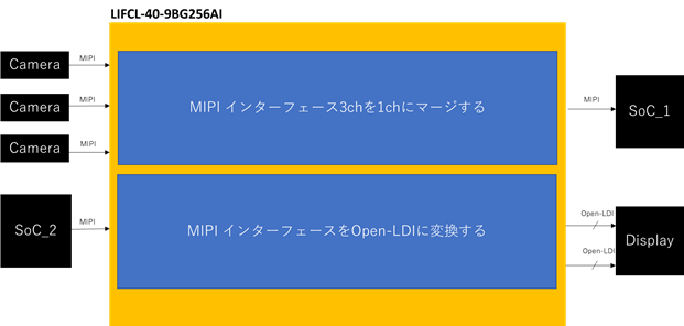
Step 2. Macnica posts a concrete configuration plan realized with FPGA
Next, Macnica will consider the resources necessary to realize your request. There are various resources to consider, but the following three are the main ones.
・Selection of IP (Intellectual Property)
・Size of LUT (Look Up Table)
・Number of I/0 (Input / Output) pins
Once the general resources have been determined, FPGA I will create an internal circuit configuration plan. First, prepare a rough configuration plan, and then discuss the details while conducting additional hearings as necessary.
I'm going to make it. around as much as possible I C and devised to have a simple structure.
Initial configuration example
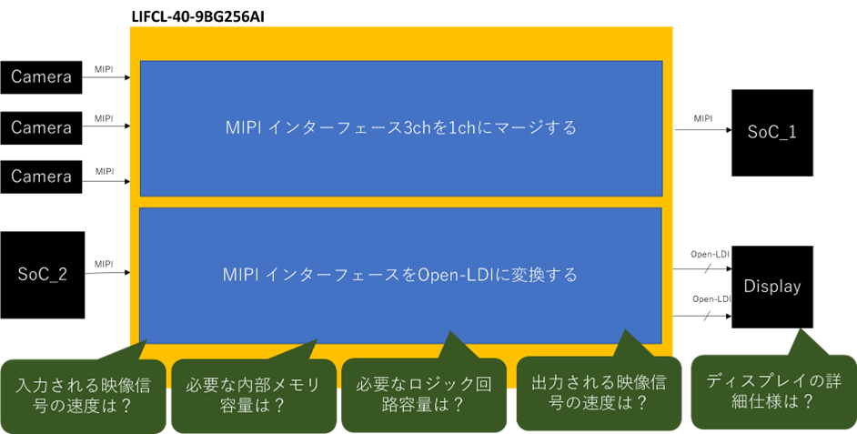
the orange part FPGA This is an internal circuit configuration plan. We proceeded with the creation while listening to the customer for additional content like a green speech bubble, and finally the content we heard
We will present several patterns of configuration proposals that can all be realized.
Step 3. Additional Proposals for Benefits Utilizing FPGA's Strengths
In addition to incorporating peripheral ICs, we also propose additional processing that takes advantage of the benefits of FPGA. Maximize the performance of the FPGA in line with the in-vehicle products you plan to use,
We will support you to get cost benefits from the introduction. We will also create and present several patterns of configuration proposals with additional benefits.
■ Examples of additional proposals
・Built-in Freeze detection function
・ Built-in local dimming function
・ Improved latency
・ Improved frame rate
Step 4. Confirmation of FPGA model number and posting of approximate price
We will select an FPGA that matches the configuration plan created in steps "2" and "3", and calculate and present an approximate price for the FPGA. At that time, we will also inform you of the model number and specifications of the FPGA you plan to use.
We offer a wide variety of configuration proposals, including low cost, low power consumption, many additional proposals, and small size.
We will select the most suitable device by considering the one that suits the in-vehicle product you plan to use, the budget, etc. By the way, in some cases, the use of IP and design tools incurs costs.
In that case, we will give you an approximate price that includes those prices. Please note that IP and design tools may be free to use, and may or may not incur costs for each proposed configuration.
Step 5. Display FPGA design development cost and period
Step "Four” is the final decision, and we have partnered with FPGA We will work out the details in cooperation with the contracted development vendor.
After that, FPGA Estimate all costs for design and development, FPGA We will provide you with a time frame for delivery.
As the “content of the estimate”, the final use FPGA and an estimate of required resources, plus an estimate of power consumption, FPGA Combined cost estimate for design and development of
becomes. If you can agree on the proposed estimate and period, follow the flow below. FPGA We will proceed with the design and development of
Although it depends on the content of the contract, in addition to the simulation verification, we also borrow the customer's actual device and undertake operation check and verification on the actual device as an FPGA contract development vendor, so please leave it to us with peace of mind. We also provide after-sales support after delivery.
■ FPGA design and development flow
[1] Formulation of specifications
[2] Preparation of specifications
[3] Logic development
[4] Logic simulation verification
[5] Implementation verification (optional)
[6] Delivery of deliverables
Key points in selecting an FPGA and creating a configuration plan at Macnica
Finally, we will introduce the key points of how Macnica selects the optimal “FPGA” and creates configuration plans with added value.
By combining IP and self-made circuits, FPGAs can realize original ICs that meet customer needs with relatively few man-hours and costs.
It is also an opportunity for designers to show their skills in deciding which FPGAs to use and what kind of combinations to propose. We listen to the needs of our customers and make full use of our knowledge and experience.
Example of FPGA configuration plan including added value related to image processing
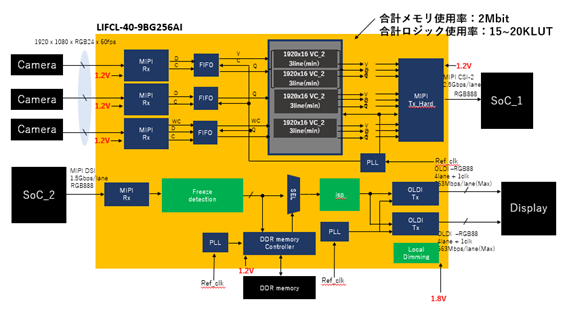
Orange part: FPGA circuit configuration
Dark blue circuit block part: IP part
Gray circuit block part: original logic circuit part
Green circuit block: Added value proposed by Macnica
For example, to create the above configuration plan, the following steps [1] to [6] are necessary, and careful consideration and confirmation are essential at each step.
We hope you will consider consulting us after learning about what Macnica actually does when it comes to FPGA consideration and implementation support.
[1] Examination of detailed specifications of FPGA input/output I/F and feasibility study
First, when choosing the most suitable FPGA, we compare the detailed specifications of the input/output I/F section with the specifications of the FPGAs used by Macnica, and consider whether the customer's request can be realized in the first place.
There are several hundred different types of FPGAs, so this is a job that requires extensive knowledge and experience.
Also, at that time, we will confirm whether IP for FPGA is available or whether it is necessary to design an original logic circuit.
[2] Consider the required number of power supply systems and I/O pin assignments
Next, check the number of power supply systems and power supply voltage. The power supply voltage to be supplied differs depending on the input/output I/F, so check whether the number of I/O pins is sufficient, and whether the I/O specifications satisfy the customer's specifications. We will narrow down the FPGA to be used while checking carefully.
[3] Consideration of FPGA internal circuit configuration
We will also consider how to mix and match PLLs, RAMs, FIFOs, and other logic. Depending on the combination of internal circuit configurations, the logic capacity used can be reduced,
It is also possible to reduce power consumption. In cooperation with FPGA development vendors, we consider multiple types of configuration plans according to FPGA resources such as LUT, RAM, and DSP.
At the same time, make a list of IPs that will be required other than the input/output I/F, and calculate the approximate value of the required internal logic capacity.
[4] Confirmation of each clock frequency
It also calculates the memory capacity required for the FPGA's internal circuitry. Examining the clock system for supplying PLL, RAM, FIFO, and other logic,
Consider various clock frequencies. In addition to calculating various clock frequencies, FPGA Internal operating frequency, whether it can be generated internally, and even on the actual design tool
We will confirm. Later, I selected it at Macnica. FPGA Careful checks are essential to avoid situations where we are unable to support frequencies that suit customer specifications.
If necessary, you can also use the power consumption calculator at this time to calculate approximate power consumption.
[5] Selection of FPGA
Select the optimal FPGA based on [1] to [4].
As explained above, selecting an FPGA requires various considerations and investigations. Specifically, the number of I/Os, interface support, logic capacity, internal memory usage rate,
At a minimum, it is necessary to check whether internal operating frequency is supported, whether it is compatible with in-vehicle quality, whether IP is provided, confirmation of track record, and calculation of power consumption.
It would take a huge amount of time and man-hours to do it on your own, so Macnica supports all of this based on our past track record and experience.
[6] Examination of added value and additional functions
Once you have selected an FPGA, we will propose added value that meets your needs so that you can maximize the benefits of the FPGA you use.
For example, in the diagram above, the green circuit block is the value-added part. FPGA Image processing (isp), a safety mechanism circuit (Freeze detection), Local dimming Added.
We will be able to propose added value and additional functions based on our support experience, and if we can ask you about the issues in advance, we can also make proposals that will lead to problem-solving depending on the case.
We hope that you understand Macnica 's free support.
What is important at every step is to face the customer's issues and specifications, and consider them from a consistent perspective. For example, do you want to reduce power consumption?
Do you want to aim for early introduction, or do you want to improve functionality with added value and functions? The details to be considered at each step will vary depending on what is important.
We always think about the production of proposal examples that are easier to benefit from, with the customer's request as the first priority.
Another strength of Macnica is that it can broaden its proposal examples by obtaining information from collaborative partners and IP vendors.
Summary
In this article, we introduced Macnica 's free support for considering and implementing FPGAs. Support will proceed in steps 1-5 below.
``The only thing that the customer needs to prepare is a simple text summary of the requirements needed in Step 1.'' We provide support in a way that minimizes customer effort.
Step 1: Hearing about the functions you want to achieve and the issues with the existing system
Step 2: Macnica will post a detailed configuration plan for FPGA implementation
Step 3 Proposing additional benefits that leverage the strengths of FPGA
Step 4 Confirmation of FPGA model number and posting of approximate price
Step 5 Posting FPGA design and development costs and period
We also introduced key points about how Macnica selects the optimal FPGA and creates configuration plans with added value. At every step, we make it a point to consider the customer's issues and the realization of specifications, and to think of examples of proposals that are more likely to yield benefits. Another strength of Macnica is its ability to gather information from outside sources and present a wide range of proposal examples.
If you have any concerns or concerns about considering or implementing FPGAs, please feel free to contact Macnica.
If you have any questions regarding this article, please contact us below.