- 半導体事業HOME
- マクニカの製品・サービス
-
技術情報

-
イベント・セミナー
- 取扱メーカー
- サポート
- お問い合わせ
- 製品購入はこちら
- 半導体事業のメルマガ登録
![]()
![]() 条件を指定して絞り込む
条件を指定して絞り込む
現在2168件がヒットしています。check
プリンター設計者必見!低消費小型FPGAでの付加価値まとめ
本記事では、プリンターを設計している方を対象に、低消費・小型なLatticeのFPGAを用いたソリューションを紹介していきます。
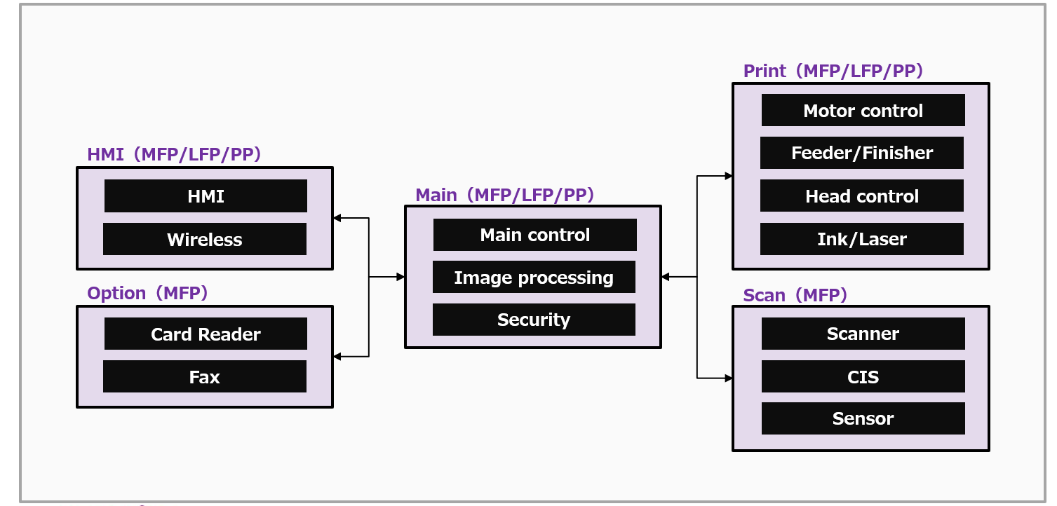
下記のように、プリンターの構成を大まかに、
Ⅰ. メイン処理部
Ⅱ. プリント部
Ⅲ. スキャン部
Ⅳ. HMI部
Ⅴ. オプション部
と分け、それぞれの機能ブロックごとに最適なソリューションを紹介していきますので、是非現在ご設計されている内容に合わせてご覧ください!
Ⅰ. メイン処理部
メイン処理部では、下記の3つのソリューションをご紹介します。
1. 電源シーケンス管理が必要なSoCやCPUに対して、小型FPGAで電源監視および電源シーケンス制御
2. バス接続などでIOが不足しているASICやCPUに対して、小型FPGAでIO拡張やレベルシフト
3. NISTなどSecurityの対応が求められる基板に対して、Securityエンジンをハードで搭載した小型FPGAでSecure bootの構成を構築
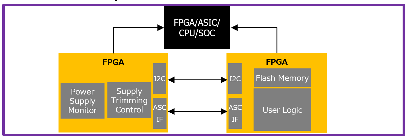
Ⅰ-1. 電源監視および電源シーケンス制御
・ディスクリート回路による電源監視機構をIC化することで、基板の面積削減に貢献
・6~12chのマルチ電源監視ポートを持ち、トリップポイントの設定数は368ポイント、15~20mv単位での高精度監視が可能
・電源異常やその兆候を検知し、内容を記録する事で故障時の解析に役立てることが可能
Ⅰ-2. IO拡張/レベルシフト
・小型、低消費、低コストのFPGAでASICやCPUのポート不足を解消
・電圧レベルが合わないIC間での電圧レベルを調整
・Latticeでは3.3V単一電源駆動が可能なFlash内蔵の1chip型FPGAでまとめて実現可能
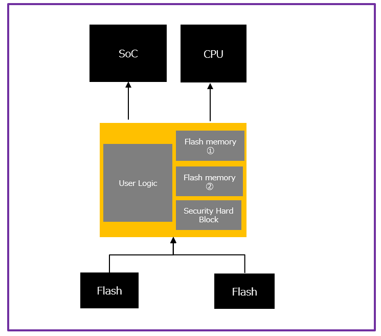
Ⅰ-3. Securityエンジンをハードで搭載した小型FPGAでSecure boot
NIST 800-193で求められる下記機能を小型FPGAで実現
・Protection:コンフィグデータを署名
・Detection:XO3Dが署名を検証
・Recovery:検証後、不備があれば別フラッシュからブート開始
↓↓↓詳細資料はページ下部からダウンロードできます↓↓↓
Ⅱ. プリント部
プリント部では、下記の5つのソリューションをご紹介します。
1. Stepping Mmotorの複数軸同期制御
2. Servo motorのFOC制御
3. Head基板制御とADC
4. Ink/Laser基板等の複数基板間の通信
5. 基板間通信のケーブルを省配線化
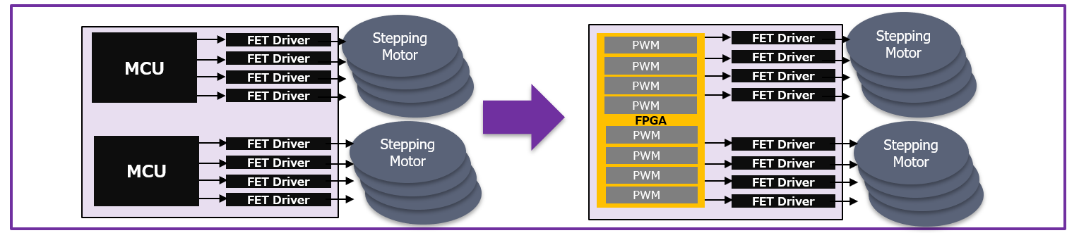
Ⅱ-1. Stepping Mmotorの複数軸同期制御
並列処理可能なFPGAの特徴を生かしてPWM出力し、複数軸を1Chipで高精度に制御
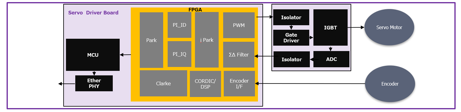
Ⅱ-2. Servo MotorのFOC制御
・電流ループ演算をMCUからFPGAに任せることで精度向上が可能
・Park変換やClarke変換等のライブラリを提供
・エンコーダーI/Fの取りまとめやフィルター回路などもまとめて実装可能
・これらの処理をLatticeでは最小10mm角のパッケージで実現可能
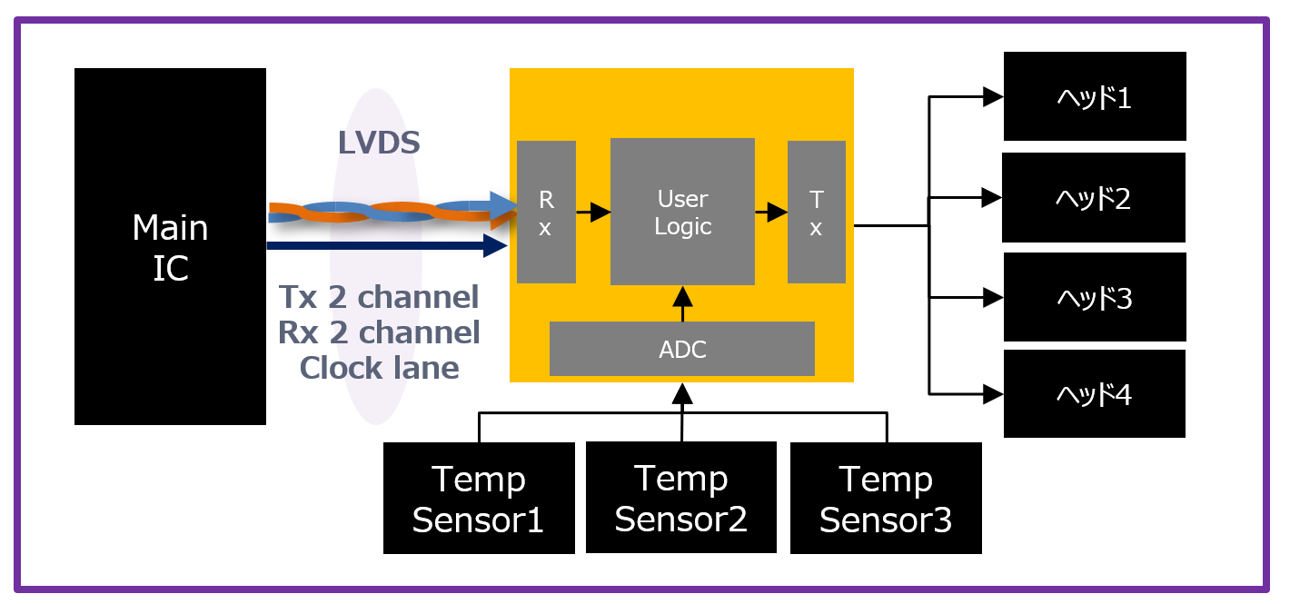
Ⅱ-3. Head基板制御とADC
・小型で低消費電力なFPGAで発熱を抑えながら同時に複数のHead基板を制御
・温度センサーのアナログ信号を内蔵ADCで監視
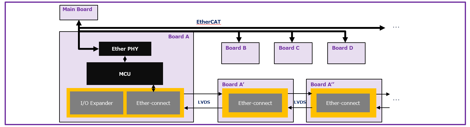
Ⅱ-4. Ink/Laser基板等の複数基板間の通信
・低コストで小型なFPGAで末端基板増設などの要求に柔軟に対応
・基板上のMCUの補助としてロジックICの取りまとめやIO拡張といった機能も取り込むことが可能
・LatticeからEther-connectのリファレンスデザインを提供可能
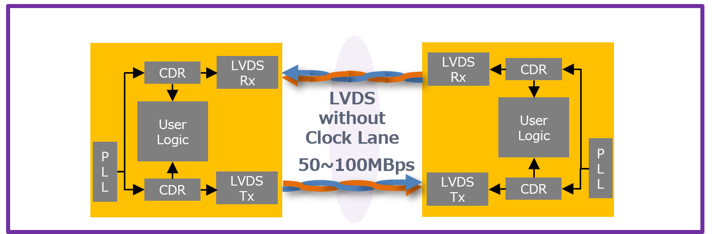
Ⅱ-5. 基板間通信のケーブルを省配線化
・LVDSのClock Laneを排除し通信を行うことによって省配線化
・Data/Clock間のSkewが発生しない
↓↓↓詳細資料はページ下部からダウンロードできます↓↓↓
Ⅲ. スキャン部
スキャン部では、下記の2つのソリューションをご紹介します。
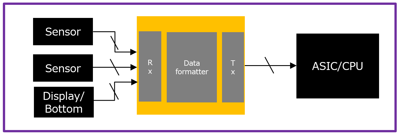
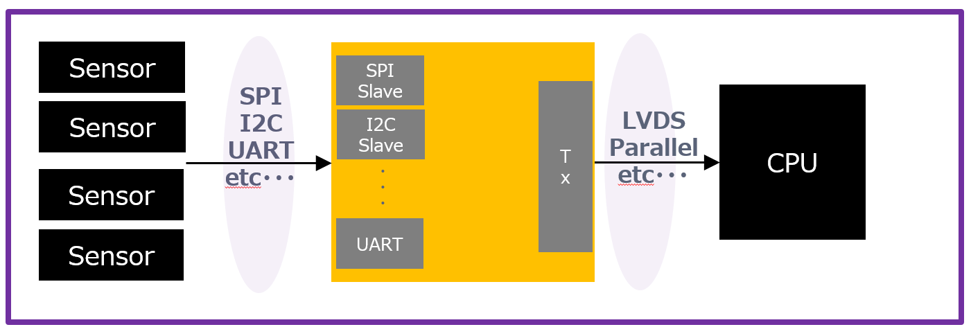
1. Sensor IFの取りまとめ
2. Channel Linkの取りまとめ
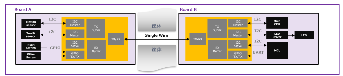
Ⅲ-1. Sensor IFの取りまとめ
・I2C, UART, GPIOの複数チャンネルを取りまとめ、一本のワイヤーで送受信
・最大7チャンネルまで取りまとめが可能 (トータルデータレートは7.5Mbps以下)
・I2Cは100Kbps, 400Kbps[Fast-Mode], 1Mbps[Fast-Mode Plus]をサポート
・GPIOは1チャンネルあたり、最大16bitかつ2Mbpsの送受信が可能
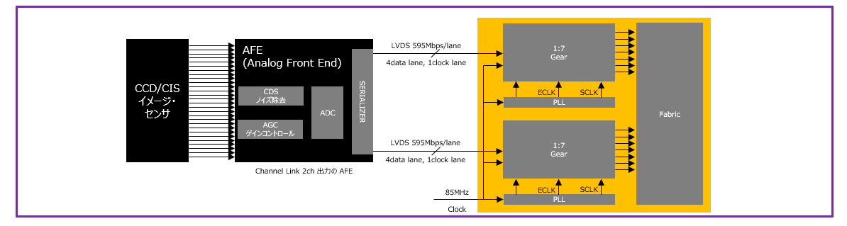
Ⅲ-2. Channel Linkの取りまとめ
・CCD, CISイメージセンサーからAFEを経由して出力されるChannel Linkを、小型低消費FPGAで受信可能
・ハードマクロにより1:7のDeserializeを1チップで実現可能
↓↓↓詳細資料はページ下部からダウンロードできます↓↓↓
Ⅳ. HMI部
HMI部では、下記の2つのソリューションをご紹介します。
1. 映像 IFの取りまとめ
2. Wifi Module IFの取りまとめ
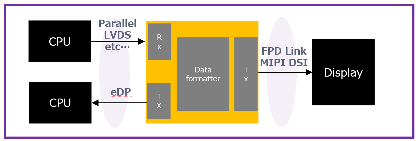
Ⅳ-1. 映像 IFの取りまとめ
・Display IF(FPD LinkやMIPI DSI)の変換とSerDes(PCIeやeDP)でのMain基板への伝送
・Latticeは最小10x10mmのFPGAで実現可能
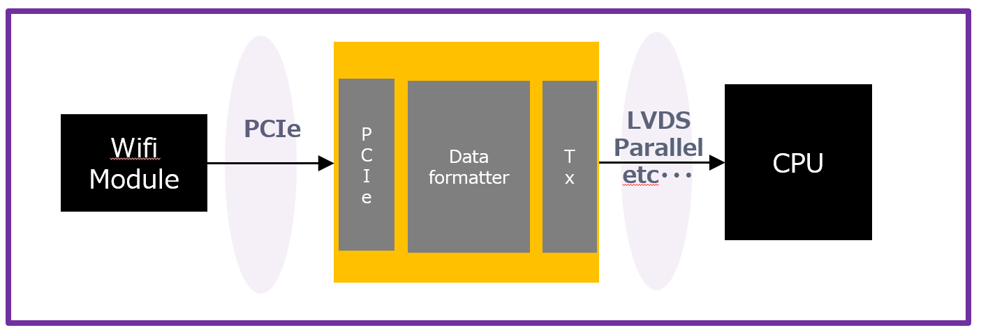
Ⅳ-2. Wifi Module IFの取りまとめ
CPUでPCIeの制御とデータ処理を行うと負荷が大きくなってしまうため、小型低消費FPGAを用いることでCPUの負荷を削減可能
↓↓↓詳細資料はページ下部からダウンロードできます↓↓↓
Ⅴ.オプション部
オプション部では、下記の2つのソリューションをご紹介します。
1. ロジックICの取りまとめ
2. エッジAIの活用
Ⅴ-1. ロジックICの取りまとめ
FAXやCard Readerで使用される複数のSensor IFを取りまとめ制御
・小型FPGAによるAI処理によって、ジェスチャー検知、音声認識、人感検知を行うことが可能
・Lattice FPGAによる圧倒的な低消費電力AIソリューションで実現
関連情報
資料ダウンロード
これらのソリューションが実現できる具体的な製品名や、パッケージラインナップについても知りたい方は、下記の資料により詳しい情報を記載してあります。合わせてぜひご覧ください!
お問い合わせ
本記事に関してご質問などありましたら、以下より問い合わせください。
各種情報一覧
Lattice関連の技術情報、セミナー情報、FAQなど気になるページがありましたら、以下をクリックください。