- Semiconductor BusinessHOME
- Products and Services of Macnica,Inc.
-
technical information

-
Events and Seminars
- Handling Manufacturer
- Support
- Inquiry
- Click here to purchase products
- Semiconductor business e-mail magazine registration
![]()
![]() Narrow down by specifying conditions
Narrow down by specifying conditions
現在2178件がヒットしています。check
3 examples of solving problems with FPGA in VR / MR / AR / HMD hardware development
Since 2016, the first year of VR, products such as VR / MR / AR / HMD have been active not only for consumers such as games, but also for educational use at factories and other sites, previews of real estate properties, driving simulators, etc. B Applications for to B are also expanding. Against this background, the requirements for VR/MR/AR/HMD hardware development are also diversifying.
As we narrow down the functions to meet various needs, there are times when commercially available ICs or our own SoCs are not enough. However, FPGAs may be able to solve requests that cannot be met with SoCs or dedicated chips.
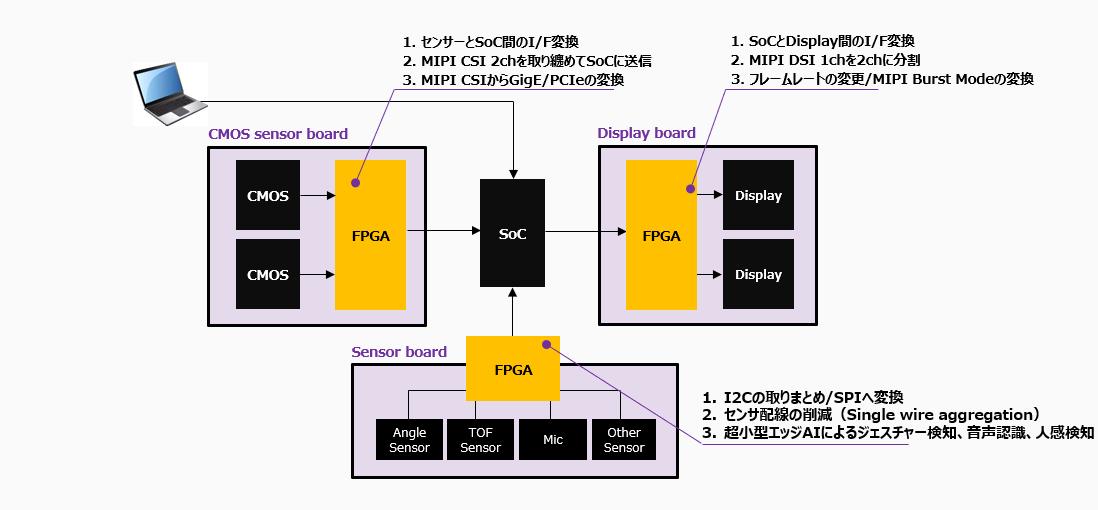
Below are typical configurations of VR/MR/AR/HMD and examples of FPGA solutions to the issues assumed for each board. Image data is input from the CMOS Sensor Board to the SoC and ISP, image processing is performed, and output to the Display Board. Depending on the model, it is assumed that there are boards that handle various inputs such as TOF sensors and microphones.
In this article, we have picked up some of the most requested solutions from this solution example. If you read to the end, you can use it as a hint to solve the following problems.
1. The SoC, sensor, and display I/F you want to use do not match
2. I want to reduce the board area
3. I want to incorporate AI, but I'm worried about the high power consumption and heat generation
Please take a look to the end!
1. The SoC, sensor, and display I/F you want to use do not match
When the I/F of the sensor/display you want to use and the SoC you are using do not match, adding an FPGA rather than changing the sensor or SoC may provide advantages in terms of both functionality and cost.
The reason for this is that not only I/F conversion is a function of FPGA, but also data format conversion (RAW10, YUV422, RGB888), which is difficult to achieve with a dedicated chip, can be realized with a single chip, so sensors and SoC because there are more options for
Also, even if the amount of data to be handled increases, some Lattice FPGAs can support signals with a MIPI rate of up to 2.5 Gbps/lane, so 4K resolution is also possible. The ability to handle such high-resolution video data is one of the appeals of FPGAs, which is difficult to achieve with dedicated chips.
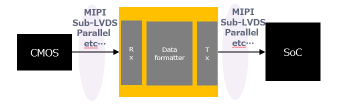
Example 1: Bridge the CMOS sensor I/F to match the later SoC I/F
・Supports various I/F such as MIPI, LVDS, Sub-LVDS, Parallel, SLVS200
・Mode conversion, frame rate change, etc. are also supported
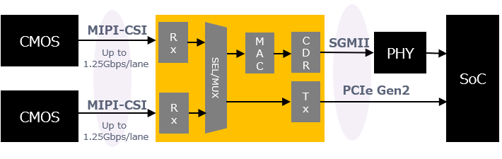
Example 2: Combine MIPI inputs and output to the subsequent SoC via GigE or PCIe
・Using FPGA hardware macros (MIPI Hard D-PHY, PCIe Hard IP, SGMII I/F)
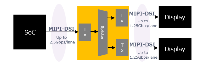
Example 3: Branch MIPI I/F 1ch to MIPI I/F 2ch and output to Display
2. I want to reduce the board area
Lattice's FPGAs include 2.5mm square small FPGAs and FPGAs that have a built-in Flash ROM for configuration and can be driven by a single 3.3V. In order to reduce the board area and downsize the housing, how about using such an FPGA to organize the wiring of the sensor?
Lattice's FPGA can provide a reference design that multiplexes signals with a small FPGA and transmits and receives on a single line. This makes it possible to save space, and if cables, connectors, and harnesses are costly, they can be replaced with FPGAs, so it is possible to reduce the board size while keeping costs down.
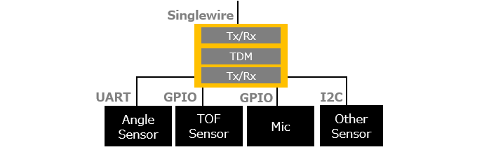
Collect multiple channels of UART, GPIO, I2C and communicate with Single wire
3. I want to incorporate AI, but I'm worried about the high power consumption and heat generation
If you try to use AI when considering new added value that is not available in other companies' products, in the case of products that must be battery-powered or products that cannot take cooling measures such as fans, power consumption is an issue. I think there are many cases where it is difficult to implement.
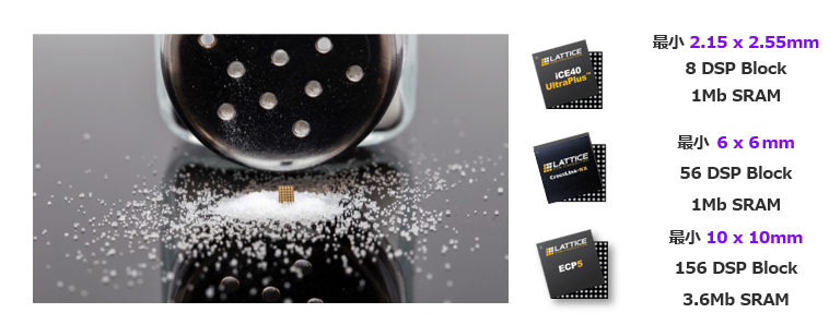
In such cases, incorporating AI inference engine IP into Lattice's FPGA can be very beneficial. This is because Lattice's AI enables implementation with a power consumption of only 1mW to less than 1W. In addition, AI processing is possible even in an ultra-small package of 2.15 x 2.55 mm, so it can be mounted without problems even if the case is small.
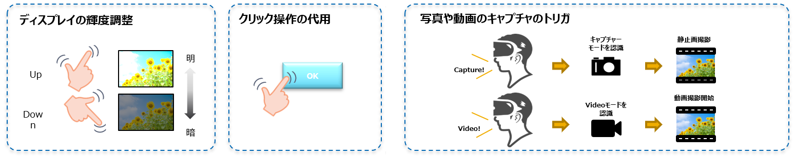
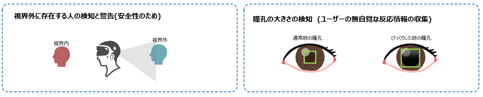
Even with such small and low-consumption AI processing, it is possible to perform gesture detection, voice recognition, human detection, etc. For example, you can use it as follows, so if you are interested, please contact us. We will strongly support you from the AI implementation method.
Related Information
Document download
For those who want to know the specific product names and package lineup that can realize these solutions, detailed information is provided in the following materials. As mentioned at the beginning, the example introduced in this article is an example, so there are various other solutions. Please take a look at it!
Inquiry
If you have any questions regarding this article, please contact us below.
Various information list
If you are interested in Lattice-related technical information, seminar information, FAQ, etc., please click below.