- Semiconductor BusinessHOME
- Products and Services of Macnica,Inc.
-
technical information

-
Events and Seminars
- Handling Manufacturer
- Support
- Inquiry
- Click here to purchase products
- Semiconductor business e-mail magazine registration
![]()
![]() Narrow down by specifying conditions
Narrow down by specifying conditions
現在2182件がヒットしています。check

Introduction
Nice to meet you, I'm Kurami, a newcomer.
I was mainly in charge of FPGA-related articles together with Nami.
Focusing on what I didn't understand and what I wondered during the production practice,
I would like to write various articles about FPGA, so please look forward to it.
In this production practice, Intel (formerly Altera) Cyclone® IV FPGA (EP4CE10E22C8) was used.
Exactly one month ago, I received a brief explanation about production practice, and started the production practice without knowing left or right.
One day, two weeks later, a question came to my mind.
"FPGA has a lot of pins, but what should be placed on which pin?"
When I asked a senior colleague, he told me that I could find out by looking at Altera's website, so I did some research. .
Explanation of pinout using Quartus® Prime
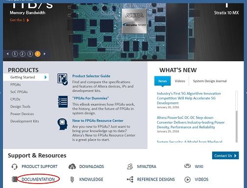
First, go to the Intel website and click DOCUMENTATION under Support & Resources.
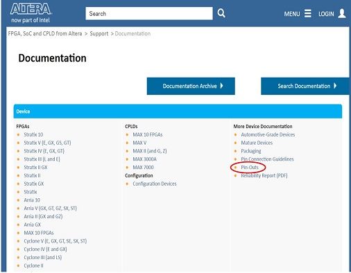
Click Pin-Outs in the More Device Documentation column.
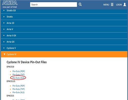
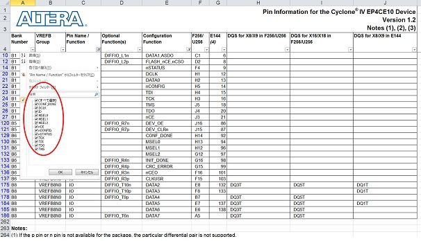
Looking at the EP4CE10 used this time, there were PDF and Excel files. I downloaded the Excel file and tried it.
If you open the file, you'll find all the information about which pin has what function...!
This sheet is easy to understand because you can check the list of dedicated pins and pins that can be used as user I/O.
Since I am using a 144-pin device this time, by comparing the pin number listed in the E144 column and the Pin NAME / Function column,
You can see which pin has what function. For example, in the example below, pin 6 is I/O,
User's favorite function can be arranged.
You can also see that pin 14 has a function called nCONFIG.
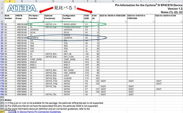
nCONFIG is a function pin that starts configuration by transitioning from LOW to HIGH, and is one of the pins related to configuration.
You can also see where other pins required for configuration such as nSTATUS, DCLK and DATA0 are located.
By the way, you can also filter with the check Box in the red frame in the figure below.
Now that we know which pins of the FPGA have what roles, we can proceed with pin placement, and that's it.
So how do I actually use Quartus Prime for pin placement?
Also, what should I do with unused pins?
Next time, I will introduce how to solve such a question.
Please also take a look at "FPGA Pin Assignment Part 2".