- Semiconductor BusinessHOME
- Products and Services of Macnica,Inc.
-
technical information

-
Events and Seminars
- Handling Manufacturer
- Support
- Inquiry
- Click here to purchase products
- Semiconductor business e-mail magazine registration
![]()
![]() Narrow down by specifying conditions
Narrow down by specifying conditions
現在2189件がヒットしています。check

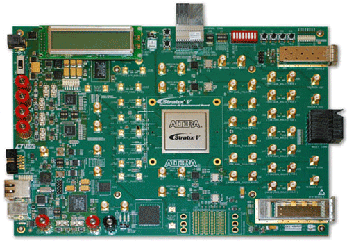
Transceiver Signal Integrity Development Kit Stratix
®V GX Edition" is the best board for FPGA design and verification that handles high-speed signals. With access to multiple channels, designers can perform real-world system analysis using on-board SMA connectors and industry-favorite backplane connectors.

Evaluate transceiver link performance from 600 Mbps to 12.5 Gpbs
Easy-to-use GUI (no Quartus ® II required) to generate and check PRBS patterns
Fine tune link settings for optimal bit error ratio (BER) with advanced equalization capabilities
Jitter analysis
10GbE, 10GBASE-KR, PCI Express (Gen1, Gen2, and Gen3), Serial Rapid IO, Gigabit Ethernet, 10 Gigabit Ethernet XAUI,
Validate PMA compliance with CEI-6G, CEI-11G, SerialRapidIO, HD-SDI, Interlaken, and other key standards
Evaluate custom backplane performance and link BER using high speed backplane connectors
Contents of the development kit
| product name | Transceiver Signal Integrity Development Kit Stratix V GX Edition |
| order number | DK-SI-5SGX230N |
| On-board device | 5SGXEA7N2F40C2NES |
Stratix V GX Development Board
On-board device
・ 5SGXEA7N2F40C2NES (622,000 LE)
Configuration and setup
・Environment
・JTAG
・ Next-generation embedded USB blaster (USB blaster 2.0)
・ FPP configuration with MAX ® II device and flash memory
- Stores two configuration files
・ Temperature measurement circuit (die and ambient temperature)
clock
- 50MHz, 125MHz, programmable oscillator (preset values: 624MHz, 644.5MHz, 706.25MHz, 875MHz)
- SMA connector for supplying an external differential clock to the transceiver reference clock
・ SMA connector for supplying external differential clock to FPGA fabric
・ SMA connector for outputting a differential clock from the PLL (Phase-Locked Loop) output pin of the FPGA
General purpose user input/output
10/100/1000Mbps Ethernet PHY (SGMII) with RJ-45 (copper) connector
・ 16x2 character LCD
- One 8-position DIP switch
- 8 user LEDs
- 4 user pushbuttons
memory device
128 Mbytes of synchronous flash memory (used to store FPGA configuration data)
High speed serial interface
7 full-duplex transceiver channels routed to SMA connectors
- Short traces on micro strip
6 stripline channels from the same transceiver block (all trace lengths match between channels)
21 full-duplex transceiver channels routed to backplane connectors
・ 7 channels to Molex ® connectors
・ 7 channels to Amphenol ® XCede ®
7 channels to Tyco Strada ® Whisper ® connector footprint
power supply
・ Laptop DC power input
・ Voltage margining
Stratix V GX Transceiver Signal Integrity Development Kit Software Contents
Altera's complete design suite (download from the Altera Download Center)
- Quartus II software supports Stratix V FPGAs
・ 1 year license included
・ Nios ® II Embedded Design Suite
・ PCI Express, Triple Speed Ethernet, SDI, and DDR3 High Performance Controller MegaCore ® MegaCore with IP core ® IP library
・ IP evaluation via OpenCore Plus is also available
Board Update Portal
Equipped with Nios II web server and remote system updates
GUI based board test system
・ Interface to PC via JTAG
- User controllable PMA settings (pre-emphasis, equalization, etc.)
・ Status display (error, BER, etc.)
complete documentation set
User guide
Reference manual
Board schematic and layout design files
Related Documents
| Document | explanation |
| User Guide(English/PDF) | Learn how to set up the Stratix V GX Transceiver Signal Integrity Development Board and use the included software. |
| Reference ManualPDF) | Contains details about the board's components and interfaces. |
| Kit installation(PDF) | Installation of all files included in the development kit including reference manuals, user guides, quick start guides, bill of materials, layouts, PCBs, schematics, signal integrity demos, board update portal example files, etc. |