- Semiconductor BusinessHOME
- Products and Services of Macnica,Inc.
-
technical information

-
Events and Seminars
- Handling Manufacturer
- Support
- Inquiry
- Click here to purchase products
- Semiconductor business e-mail magazine registration
![]()
![]() Narrow down by specifying conditions
Narrow down by specifying conditions
現在2186件がヒットしています。check

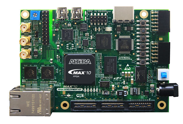
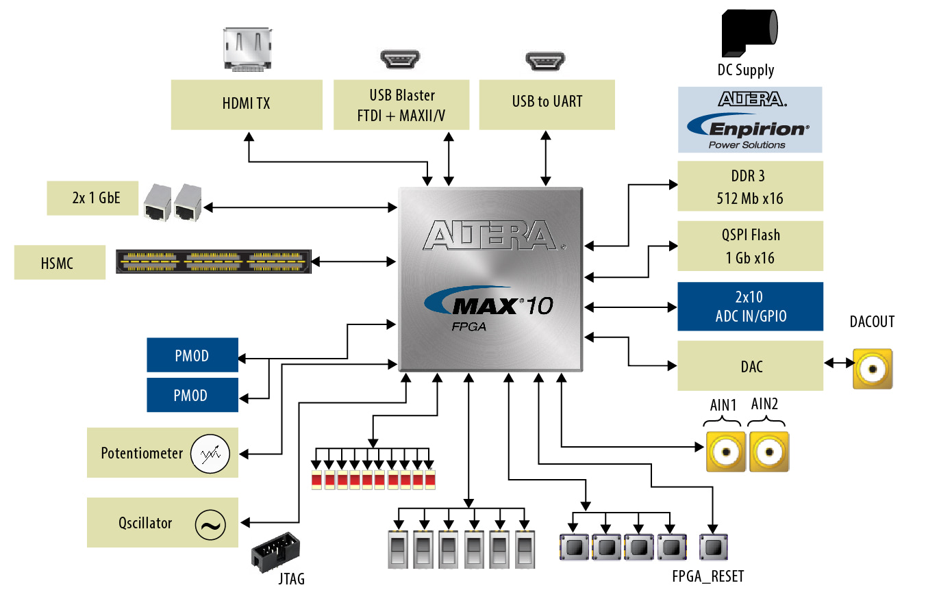
The Intel MAX 10 FPGA Development Kit is optimized for system-level integration with support for an on-die analog-to-digital converter (ADC), dual configuration flash memory, and DDR3 memory interfaces. A full-featured design platform with a 50,000 logic element (LE) MAX 10 FPGA.
With onboard USB-Blaster™ II, High Speed Mezzanine Card (HSMC), Pmod™ compatible expansion card, HDMI output, and dual Ethernet for industrial Ethernet applications, it is ideal for industrial, automotive, consumer and many more We provide system-level prototyping solutions that are ideal for market applications.
feature
This development board allows you to:
![]() Design development targeting 10M50D, F484 package FPGA
Design development targeting 10M50D, F484 package FPGA
![]() Measuring Digital Conversion Performance of Analog Blocks in MAX 10 FPGAs
Measuring Digital Conversion Performance of Analog Blocks in MAX 10 FPGAs
![]() 300 MHz interface between MAX 10 FPGA and DDR3 memory
300 MHz interface between MAX 10 FPGA and DDR3 memory
![]() Nios® II processor running embedded Linux
Nios® II processor running embedded Linux
![]() HSMC and Digilent Pmod™ compatible connectors for interfacing to daughtercards and peripherals
HSMC and Digilent Pmod™ compatible connectors for interfacing to daughtercards and peripherals
![]() FPGA power (VCC_CORE and VCC_IO) measurement with power monitor GUI (Graphical User Interface)
FPGA power (VCC_CORE and VCC_IO) measurement with power monitor GUI (Graphical User Interface)
![]() Reusing PCB information and schematics as deployment models for custom designs
Reusing PCB information and schematics as deployment models for custom designs
Order information
| product name | MAX 10 FPGA Development Kit |
| order code | DK-DEV-10M50-A |
| On-board device | 10M50DAF484I6GES |
MAX 10 Development Board Contents
RoHS and CE Compliant MAX 10 FPGA Development Board
On-board device
・MAX 10 FPGA (10M50D, dual voltage, F484 package)
・4A PowerSoC Voltage Mode Synchronous Buck Converter with Enpirion ® EN2342QI Inductor
・Enpirion EN6337QA 3A High Efficiency PowerSoC DC-DC Buck Converter with Inductor
・600 mA PowerSoC DC-DC Buck Converter with Enpirion EP5358xUI Inductor
・MAX II CPLD – EPM1270M256C4N (onboard USB-Blaster II)
Programming & Configuration
・Embedded USB-Blaster II (JTAG)
・JTAG direct option (via 10-pin header)
memory device
・64Mx16 1 Gb DDR3 SDRAM (soft memory controller)
128Mx8 1 Gb DDR3 SDRAM (soft memory controller)
・512Mb 4-wire SPI flash memory
communication port
2 Gigabit Ethernet (GbE) RJ-45 ports
・1 mini-USB2.0 UART
・1 HDMI video output
- 1 generic HSMC connector (see HSMC expansion card)
Two 12-pin Digilent Pmod™ compatible connectors (see Pmod™ Compatible Expansion Cards)
analog
・MAX 10 FPGA ADC SMA input x 2
・2x10 ADC header
・Potentiometer input to ADC
One external 16-bit digital-to-analog converter (DAC) device with SMA output
clock
25 MHz single-ended external oscillator clock source
・Silicon Labs clock generator with GUI for frequency programming
Switches, Push Buttons, Jumpers, Status LEDs
Mini USB cable for onboard USB Blaster II
2A power adapter and cord
complete documentation
User manual, bill of materials, schematics, board files
Development software Quartus Prime
Download Quartus Prime Lite Edition for MAX 10 FPGA development here.

Related Documents
| Document | explanation | version |
| User guide (English edition) |
Information about the MAX 10 FPGA Development Kit hardware and board setup, including how to use the included software. | 2015.06.26 |
| Rev C Schematic (English edition) |
Board Revision C Schematic. Refer to the User Guide for how to check the board revision. | C1 |
| Rev C. Board Kit Full install (Windows PC only) |
Installation of all designs, GUIs, user manuals, bills of materials, layouts, printed circuit board documentation, schematics and other documentation/files. **For Rev C board kit only** |
15.0.0 |
| Rev B Schematic (English edition) |
Board Revision B Schematic. Refer to the user guide for how to check the board revision. | B1 |
| Rev B. Board Kit Full install (Windows PC only) |
Installation of all designs, GUIs, user manuals, bills of materials, layouts, printed circuit board documentation, schematics and other documentation/files. ** Rev B board kit only ** |
15.0.0 |
BUY MAX 10 DEVELOPMENT KIT
You can purchase the MAX 10 development kit here.