- Semiconductor BusinessHOME
- Products and Services of Macnica,Inc.
-
technical information

-
Events and Seminars
- Handling Manufacturer
- Support
- Inquiry
- Click here to purchase products
- Semiconductor business e-mail magazine registration
![]()
![]() Narrow down by specifying conditions
Narrow down by specifying conditions
現在2182件がヒットしています。check

The Cyclone ® V GX FPGA Development Kit from Intel® provides a design environment for rapid development of low-cost, low-power FPGA system-level designs.
feature
With this development kit, you can:
- FPGA prototyping
- FPGA power consumption measurement circuit
- Signal quality test for transceiver I/O up to 3.125 Gbps
- PCI Express ® (PCIe ®) x4 lanes with transfer rates up to 1,000 Mbps
- endpoint or root port
Order information
| product name | Cyclone V GX FPGA Development Kit |
| order code | DK-DEV-5CGXC7NES |
| The Cyclone V GX FPGA development kit includes 5CGX–C7-C7NES speed grade production silicon devices. | |
Contents of the development kit
The Cyclone V GX FPGA Development Kit includes:
- Cyclone V GX FPGA development board (see Figure 1)
- On-board device
- Cyclone V GX FPGA - 5CGXFC7D6F31C7NES
- MAX ® V CPLD - 5M2210ZF256C4N (System Controller)
- MAX II CPLD - EPM240M100C4N (Embedded USB-Blaster™ II)
- MAX II CPLD- EPM240M100C4N (optional, 3rd party security CPLD feature)
- Constitution
- Embedded USB-Blaster II (JTAG)
- Fast Passive Parallel (PFL)
- memory device
- 2 banks of 40-bit DDR3 SDRAM with error correction code (ECC)
- 512 MB Flash memory and 18 MB SRAM
- Standard communication port
- USB 2.0
- Gigabit Ethernet
- PCIe x4 edge connector
- General Purpose High Speed Mezzanine Card (HSMC) (4-ch Transceiver, 16-ch Tx LDVS, 16-ch Rx LVDS)
- 1 SDI channel
- Two SMA connectors per transceiver channel
- Push Buttons, DIP Switches, and LEDs
- clock
- Programmable clock generator for FPGA reference clock input
- 125 MHz LVDS oscillator for FPGA reference clock input
- 148.5/148.35 MHz LVDS VCXO for FPGA reference clock input
- 50 MHz single-ended oscillator for FPGA and MAX V FPGA clock input
- 100 MHz single-ended oscillator for MAX V FPGA configuration clock input
- SMA input (LVPECL)
- power supply
- Laptop DC power input adapter (14-20V)
- PCIe edge connector
- System monitor circuit
- Power (voltage, current, wattage)
- housing
- PCIe card standard size (6.600" x 4.199")
- On-board device
- Cyclone V GX FPGA Development Kit Software Contents (downloadable from Table 2)
- design example
- PCIe loopback and reference designs
- Board Test System (BTS)*
- Board Update Portal (BUP)*
- Includes Nios ® II embedded soft processor and Ethernet
- This kit does not include a Quartus II development software license.
- design example
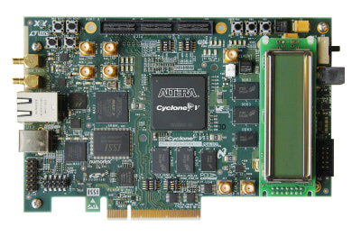
Figure 1. Cyclone V GX FPGA Development Kit
Related Documents
| document | explanation |
|
Cyclone V GX FPGA Development Kit User Guide (English / PDF) |
Learn how to set up the Cyclone V GX FPGA development board and use the included software. |
|
Cyclone V GX FPGA Development Board Reference Manual (English/PDF) |
Contains details about the board's components and interfaces. |
| Kit installation (via FTP) (coming soon) |
Full documentation of all files including reference manuals, user guides, quick start guides, bill of materials, layouts, PCBs, schematics, Board Update Portal example files, Board Test System example files, etc. install. The board update portal has been upgraded to Qsys. |