- Semiconductor BusinessHOME
- Products and Services of Macnica,Inc.
-
technical information

-
Events and Seminars
- Handling Manufacturer
- Support
- Inquiry
- Click here to purchase products
- Semiconductor business e-mail magazine registration
![]()
![]() Narrow down by specifying conditions
Narrow down by specifying conditions
現在2186件がヒットしています。check

The Intel® Arria® V GX Starter Development Kit provides a complete design environment that includes all the hardware and software needed to rapidly develop cost-sensitive FPGA applications. This development kit is RoHS compliant.
feature
This development kit has the following features:
- Arria V GX FPGA - Approximately 360,000 equivalent logic elements, F1152 package, 24 6.5G transceivers, C5 speed grade
- 1 I/O expansion slot - 1 High Speed Mezzanine Card (HSMC) connector
- 256 MB SDRAM memory
- HDMI and SDI connectors
- SMA connector
Order information
| product name | Arria V GX Starter Development Kit |
| order code | DK-START-5AGXB3NES |
| The Arria V GX Starter Development Kit features a 5AGXB3 Engineering Sample (ES) device and includes a one-year license for Quartus® II development software. | |
Contents of the development kit
The Arria V GX Starter Development Kit includes:
- The Arria V GX Starter Development Kit includes:
- Arria V GX FPGA development board (see Figure 1)
- FPGA: Arria V GX 5AGXFB3H4F35C5NES
- System Controller: MAX ® V 5M2210ZF256C4N
- Power monitor GUI
- 1 analog-to-digital converter (ADC), 8 channels
- Non-isolated power rail
- Fast Passive Parallel (FPP) x16 Mode with Parallel Flash Loader (PFL)
- Control and status registers
- Embedded USB-Blaster™ II: MAX II EPM570GM100C4N
- HDMI 1.3 TX
- HDMI TX connector with 4 transceivers, up to 2.7 Gbps (with level shifter) and TX clock 270 MHz
- STMicroelectronics HDMI level shifter STHDLS101T
- Allows level shifting of PCML 1.5V <-> TMDS level transceivers
- DDC and HPD <-> HDMI compliant levels
- Data channel up to 2.7 Gbps per HDMI 1.3
- Clock channel up to 270 MHz to fully support 2.7 Gbps data rate
- HDMI specification: clock period = 10 times UI
- SDI 3G
- 1 transceiver TX/RX loopback
- Two SMB connectors and cables (cables not included in kit)
- Up to 2.97Gbps
- Uses National Semiconductor Driver/Receiver LMH0384SQ/LMH0303SQx
- US and EU standards support requires transceiver reference clocks of 148.5 MHz and 148.35 MHz respectively
- Fine tune using VCXO to lock to recovery CDR frequency
- HSMC
- Eight up to 6.375 Gbps transceivers
- Non-Compliant with PCI Express ® (PCIe ®) HIP Pin Assignments
- 4 CMOS
- 8 TX and 9 RX differential interfaces with dedicated TX/RX channels
- Two LVDS clock inputs
- 2 differential clock outputs
- I2C
- JTAG
- Minimum current support
- 2A @ 3.3V
- 1A @ 12V
- Dedicated clock domain for transceiver reference clock from Si 5338 clock generator
- HSMC loopback with BTS GUI
- SMAs
- 1 transceiver TX/RX channel
- 1x LVPECL clock input
- 1x LVPECL clock output
- Dedicated clock domain for transceiver reference clock from Si 5338 clock generator
- DDR3 SDRAM x32
- Micron MT41J64M16LA-15E DDR3 SDRAM 8MX16X8
- 2 devices: 2 x16 width = x32
- BTS DDR3 SDRAM GUI with UniPHY and High Performance (HP) Controller II
- SSRAM
- 512 kbit x36, 18 megabit ISSI IS61VPS51236A
- Share address or data with flash
- User I/O
- Character LCD
- 4 DIP switches
- 3 push buttons
- 4 LEDs
- Constitution
- FPP x16 mode
- Dual Flash 512 Mbit Numonyx PC28F512P30BF (52 MHz F MAX)
- JTAG ヘッダ
- Embedded USB-Blaster II
- Equipped with Cypress microcontroller CY7C68013A as USB PHY 2.0
- MAX II
- ethernet
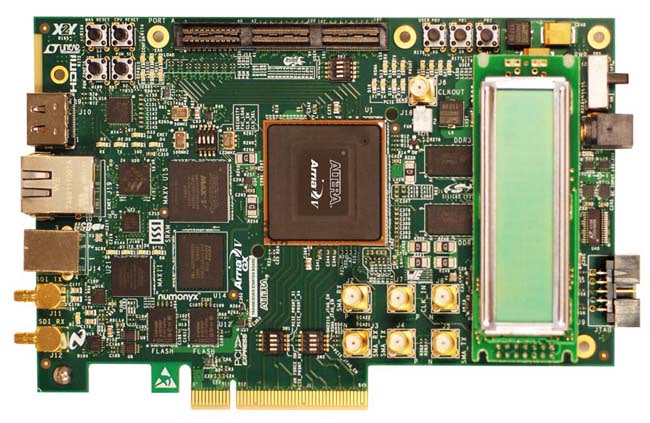
Figure 1. Arria V GX Starter Development Board
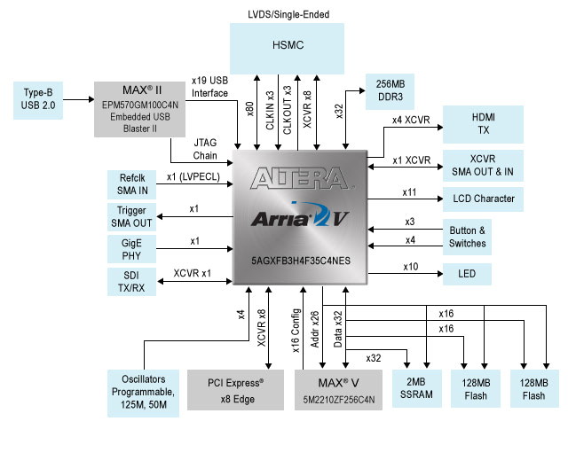
Figure 2. Arria V GX Starter Development Board Block Diagram
Related Documents
| document | explanation |
| Arria V GX Starter Development Board Reference Manual (English/PDF) | Contains details about the board's components and interfaces. |
| Arria V GX Starter Development Kit User Guide (English/PDF) | Learn how to set up the Arria V GX Starter Development Board and use the included software. |
| kit installation | Full installation of all files included in the development kit including reference manuals, user guides, quick start guides, bill of materials, layouts, PCBs, schematics, board update portal example files, etc. |