- Semiconductor BusinessHOME
- Products and Services of Macnica,Inc.
-
technical information

-
Events and Seminars
- Handling Manufacturer
- Support
- Inquiry
- Click here to purchase products
- Semiconductor business e-mail magazine registration
![]()
![]() Narrow down by specifying conditions
Narrow down by specifying conditions
現在2189件がヒットしています。check

The Intel® Arria® V GX FPGA Development Kit provides a complete design environment that includes all the hardware and software needed to develop a complete FPGA design and test it in a system environment. This development kit is RoHS compliant and has the following features:
feature
With this development kit, you can:
- 2 FPGAs for system-level design
- Arria V GX FPGA: ~360K equivalent logic elements, F1517 package, 24 6G transceivers, C5 speed grade
- 3 I/O expansion slots: 2 High Speed Mezzanine Cards (HSMC), 1 FPGA Mezzanine Card (FMC)
- 2 gigabytes of DDR3 SDRAM memory, 4.5 megabytes of QDR II+ memory, 1 gigabit of flash memory
- SFP+ connector
- SMA and Samtec Bullseye Connectors
- Ability to measure each chip's power rail independently
Order information
| product name | Arria V GX FPGA Development Kit |
| order code | DK-DEV-5AGXB3N/ES |
| The Arria V GX FPGA Development Kit features a 5AGXB3 engineering sample (ES) device and includes a one-year license for Quartus® II development software. | |
Contents of the development kit
The Arria V GX FPGA Development Kit includes:
- Arria V GX FPGA development board (see Figure 1)
- Unit 1: Arria V GX FPGA: 5AGXFB3H4F40C5NES
- memory
- 1,152-MB x72 DDR3 SDRAM
- 4.5 megabytes (1 megabit x 36) of QDR II+ SRAM
- 1 Gbit Synchronous Flash (x16)
- communication port
- PCI Express ® (PCIe ®) x8 edge connector
- HSMC Port A (4 transceiver channels)
- USB 2.0
- Gigabit Ethernet
- Chip-to-chip bridge with 29 LVDS inputs, 29 LVDS outputs, and x8 transceivers
- 1 SFP+ channel
- Bullseye connector (x1 channel)
- SMA connector (x1 channel)
- Constitution
- JTAG
- Fast Passive Parallel (FPP) Parallel Flash Loader (PFL)
- Buttons, switches, LEDs, and displays
- 1 pushbutton for configuration reset
- 1 CPU reset push button
- 3 user push buttons
- 2 push buttons for configuration
- Eight dual in-line package (DIP) switches
- 16 user LEDs (8 bicolor diodes)
- 16x2 character LCD
- memory
- Unit 2: Arria V GX FPGA: 5AGXFB3H4F40C5NES
- memory
- x64 DDR3 SDRAM soft controller (or x32 hard intellectual property (IP) controller)
- communication port
- HSMC port B (4 transceiver channels)
- FMC port (4 transceiver channels)
- Chip-to-chip bridge with 29 LVDS inputs, 29 LVDS outputs, and x8 transceivers
- 1 SDI channel
- Bullseye connector (one transceiver channel)
- SMA connector (1 transceiver channel)
- Constitution
- JTAG
- FPP PFL
- Buttons, switches, LEDs, and displays
- 1 CPU reset push button
- 3 user push buttons
- 8 DIP switches
- 16 user LEDs (8 bicolor diodes)
- memory
- Others
- EPM2210GF324 System Controller
- EPM570GM100 on-board USB-Blaster™ II download cable
- clock
- 50 MHz oscillator
- 100 MHz and 125 MHz programmable oscillators
- SMA input (LVPECL)
- power supply
- Laptop DC power input
- PCIe edge connector
- system monitor
- Power (Voltage, Current, and Wattage) ______ Unit, Rail
- Temperature (per FPGA die, local board)
Figure 1. Arria V GX FPGA Development Kit
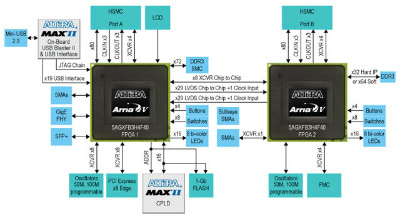
Figure 2. Arria V GX FPGA Development Kit Block Diagram
Related Documents
| document | explanation |
| Arria V GX FPGA Development Board Reference Manual (English/PDF) | Contains details about the board's components and interfaces. |
| Arria V GX FPGA Development Kit User Guide (English/PDF) | Learn how to set up the Arria V GX FPGA development board and use the included software. |
| kit installation | Install all files including reference manuals, user guides, quick start guides, bill of materials, layouts, PCBs, schematics, Board Update Portal example files, Board Test System example files, etc. |