- Semiconductor BusinessHOME
- Products and Services of Macnica,Inc.
-
technical information

-
Events and Seminars
- Handling Manufacturer
- Support
- Inquiry
- Click here to purchase products
- Semiconductor business e-mail magazine registration
![]()
![]() Narrow down by specifying conditions
Narrow down by specifying conditions
現在2176件がヒットしています。check

Interconnect for high bandwidth
A high-throughput data path between the HPS and FPGA fabric provides a level of interconnect performance not achievable with a two-chip solution.
Tight integration between the HPS and FPGA fabric enables peak bandwidths in excess of 100Gbps while maintaining integrated data coherency between the processor and FPGA. Additionally, eliminating the external I/O path between the processor and FPGA significantly reduces system power consumption.
<Excellent data integrity and wide bandwidth>
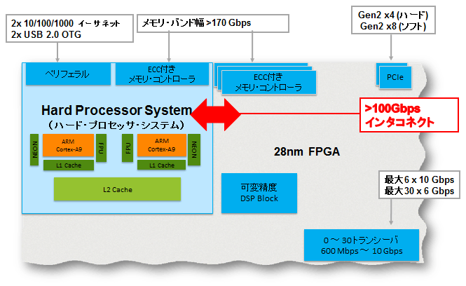
High bandwidth HPS-to-FPGA interconnect backbone
The HPS (Hard Processor System) and FPGA can operate independently, but are tightly coupled through a high-bandwidth system interconnect with a high-performance ARM AXI bus bridge. IP bus masters in the FPGA fabric can access HPS bus slaves through the FPGA-to-HPS interconnect. Similarly, HPS bus masters can access bus slaves in the FPGA fabric through the HPS-to-FPGA bridge. Both bridges are ARM AXI-3 compliant and support concurrent read/write transactions. An additional 32-bit lightweight HPS-to-FPGA bridge provides a low-latency interface between the HPS and peripherals within the FPGA fabric. Additionally, up to six FPGA masters can share the HPS SDRAM controller, and an ARM processor can be used to configure the FPGA fabric under program control through a dedicated 32-bit configuration port.
| HPS-to-FPGA | |
| Configurable 32/64/128-bit AMBA AXI interface optimized for high bandwidth | |
| FPGA-to-HPS | |
| Configurable 32/64/128-bit AMBA AXI interface optimized for high bandwidth | |
| Lightweight HPS-to-FPGA | |
| 32-bit AMBA AXI interface optimized for low latency | |
| FPGA-to-HPS SDRAM Controller | |
| Configurable multiport interface with 6 command ports, 4 64-bit read data ports, and 4 64-bit write data ports | |
| 32-bit FPGA configuration manager |