
![]()
![]() Narrow down by specifying conditions
Narrow down by specifying conditions
現在1887件がヒットしています。check

What is USB 3.1 Gen2
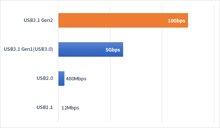
USB 3.1 Gen2 is the next-generation USB standard widely used as an interface for connecting PC peripherals.
In addition, USB3.1 Gen2 is also called "Super Speed Plus mode", enabling high-speed data communication of 10 Gbps, which is twice the communication speed (5 Gbps) of the conventional "Super Speed mode (USB 3.0)". It is
USB 3.1 Gen2 has backward compatibility, and conventional "Super Speed mode (USB 3.0)", "High Speed mode (USB2.0/480Mbps)", "Full Speed mode (USB 1.1/12 Mbps)", "Low Speed mode (USB 1.1/12 Mbps)" USB products for "Speed Mode (USB 1.0/1.5Mbps)" can also be used as is.
In recent years, the amount of data handled by USB, such as high-definition video data, has increased, and how to transfer such large-capacity data at high speed is becoming a problem. This is because the market is expected to move in the future.
By the way, with the update of the USB standard, the names have been changed as follows, but the old names are used on this page.
| USB3.2Gen2 x1 | USB3.2Gen1x2 | USB3.2Gen2x1 | USB3.2Gen2x2 | |
|
data rate |
5 Gbps |
10Gbps |
10Gbps |
20Gbps |
|
former name |
USB3.1 Gen1 or USB3.0 |
-- |
USB3.1 Gen2 |
-- |
|
connector shape |
USB-A USB-C micro USB |
USB-C only |
USB-A USB-C micro USB |
USB-C only |
Benefits of using FPGAs and how to achieve them
When implementing a USB interface, the use of ASSPs and ASICs should be considered first.
However, ASSP has limited functions, lacks versatility, and poses the risk of EOL. In addition, ASIC has major issues such as development period and high risk.
In that respect, by using FPGA, the design inside the device can be rewritten according to the user's specifications, so it is possible to solve the problem of versatility with ASSP, and FPGA has excellent supplyability. Therefore, EOL risk can be reduced.
In addition, problems such as development period and high risk, which were problems with ASIC, are greatly improved.
Then, as for the method of realizing the USB interface with FPGA, there is a method of using the transceiver block and dedicated IP installed in FPGA.
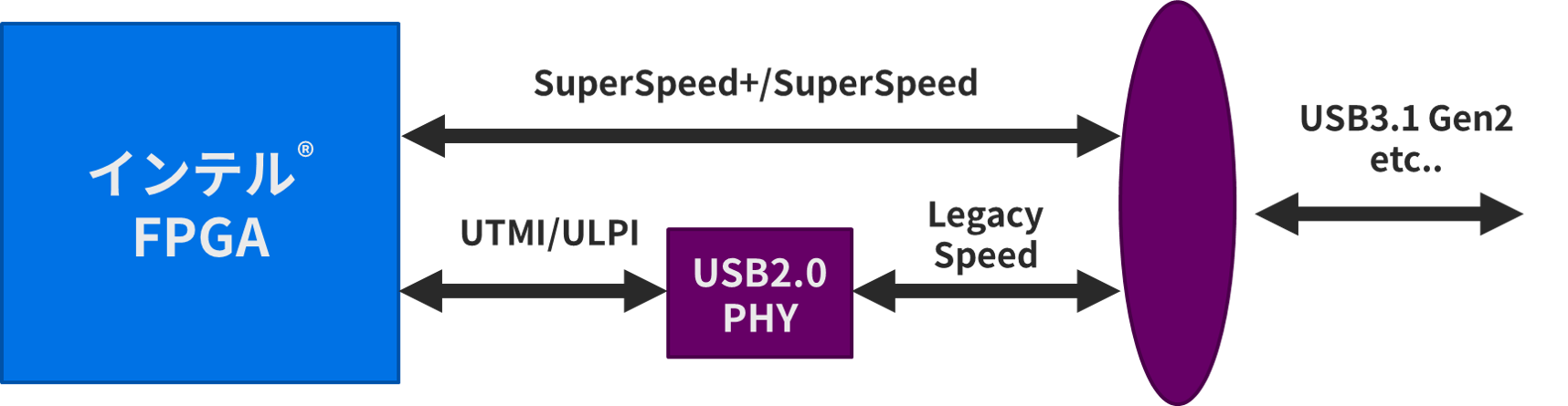
As mentioned above, USB2.0 requires an external PHY to support ULPI, but USB3.1 does not require an external PHY.
(However, we recommend using a Re-timer to ensure signal quality and a multiplexer to support Type-C double-sided connections.)
Selection of IP for realization of USB interface
As mentioned above, it is recommended to use IP to implement USB on FPGA. Currently, we are introducing the following System Level Solutions company as an IP compatible with USB3.1 Gen2.
Of course, it is also possible to support USB3.0 / 2.0 as backward compatibility.
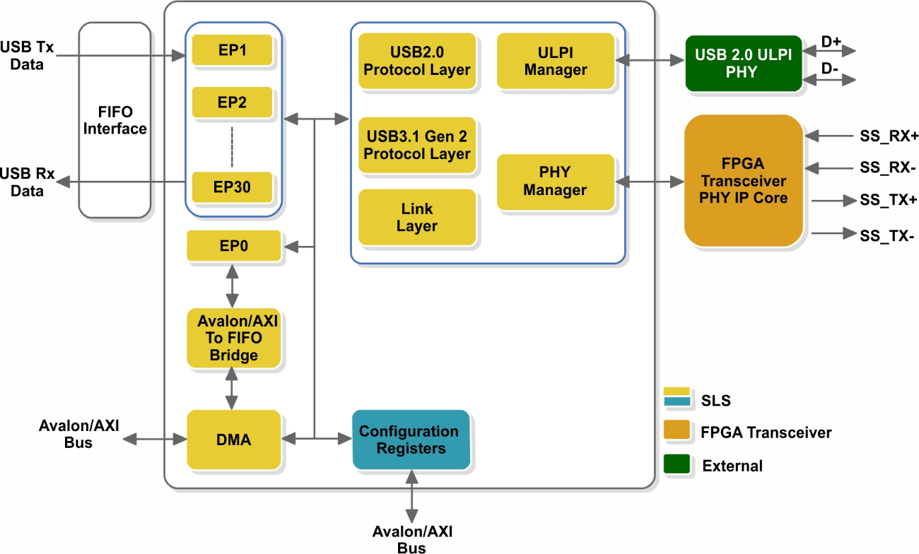
By using this IP and an Intel® Cyclone® 10 FPGA or Intel® Arria® 10 FPGA with a built-in transceiver, you can easily implement a USB interface using an FPGA.
In addition, the Intel® Cyclone® 10 GX FPGA development kit provided by Intel® has an onboard Type-C port that supports USB3.1 Gen2, so you can easily evaluate USB3.1 Gen2. is possible.
Bulk Transfer Demonstration Combining FPGA and IP
The video below shows an actual device demonstration of bulk transfer, which uses the Intel® Cyclone® 10 GX FPGA development kit and System Level Solutions IP, and is suitable for accurately transferring large amounts of data among USB transfer methods. (required time: about 3 minutes)
As you can see in this video, you can easily verify using the development kit.
Inquiry
I would like to directly ask the person in charge about the realization of a USB interface using FPGA! I want an explanation! If so, please feel free to contact us using the button below.
Intel® Programmable Solutions Group Page Top
Please click below to return to Intel® Programmable Solutions Group Page Top.