- Semiconductor BusinessHOME
- Products and Services of Macnica,Inc.
-
technical information

-
Events and Seminars
- Handling Manufacturer
- Support
- Inquiry
- Click here to purchase products
- Semiconductor business e-mail magazine registration


 Narrow down by specifying conditions
現在2169件がヒットしています。check


Introduction
Hello, I'm Mass Man.
This embarrassing story is about what I thought when I first learned about the built-in memory blocks of FPGAs.
FPGA devices have memory blocks (dedicated areas used as memory) built into them.
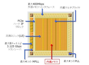
Figure 1. Internal structure of Cyclone® IV
The user can implement the following three types of memory using this memory block:
• RAM (Random Access Memory): Memory that allows data to be written to and read from a specified address. It is volatile, meaning the data is erased when the power is turned off.
ROM (Read Only Memory): A type of memory that reads data from a specified address. It is non-volatile, meaning the data remains even when the power is turned off. Data must be written to the ROM beforehand.
FIFO (First-In First-Out): A memory type that reads data in the order it was written, starting with the oldest data. It does not have the concept of addresses.
Memory blocks can be designed from the Tools menu ⇒ MegaWizard Plug-In Manager in Quartus® II.
I was surprised to learn that an FPGA's memory block can implement three types of memory (ROM, RAM, and FIFO).
That's when Masuo had an idea.
"ROM data is not erased even when the power is turned off. So, couldn't we implement ROM using an FPGA memory block, write circuit data to it, and then use that memory block as configuration memory?"
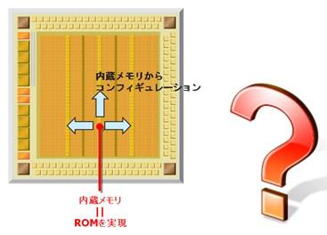
Figure 2. Masuo's blushing image
I told my senior colleague about Masuo's thoughts.
Senior employee: "FPGAs use an SRAM structure, which means the data is volatile and disappears when the power is turned off. Similarly, the built-in memory block also uses an SRAM structure. The physical structure of the memory block doesn't change to a ROM structure, you know (laughs)."
In other words, the built-in memory block had an SRAM structure, and by freely programming the presence or absence of the Write Enable signal and Address signal, it was able to operate (behave) like ROM or FIFO!
- SRAM without a write signal (Write Enable) is behaving like ROM.
- SRAM without an address signal (Address) is functioning like a FIFO.

Masuo: "I mistakenly thought the physical structure of the memory block would change (embarrassing). The beauty of FPGAs is that you can freely program whether or not the memory control signals are connected! The configuration device is non-volatile ROM, so an SRAM memory block wouldn't work."
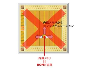
Senior employee: "Saying it can be configured with ROM is incorrect. Do you understand that there are various physical structures for ROM? Try researching the different types of memory."
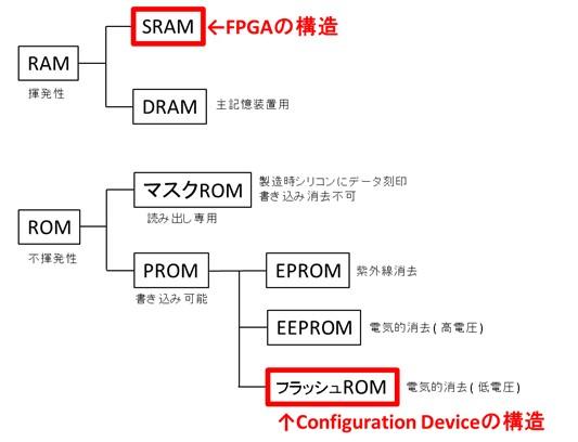
Figure 3. Types of Memory
Masuo: "So the configuration device has a flash ROM structure!"
what i learned
Altera FPGAs have built-in memory blocks that can implement RAM, ROM, and FIFO.
The built-in memory block has an SRAM structure, and the presence or absence of the Write Enable signal and Address signal can be freely programmed.
This allows it to function like a ROM or FIFO.