- Semiconductor BusinessHOME
- Products and Services of Macnica,Inc.
-
technical information

-
Events and Seminars
- Handling Manufacturer
- Support
- Inquiry
- Click here to purchase products
- Semiconductor business e-mail magazine registration
![]()
![]() Narrow down by specifying conditions
Narrow down by specifying conditions
現在2168件がヒットしています。check


Hello, I'm Mass Man.
Starting this week, part two! "Practice series of FPGA by mass man"
In the first installment of the series, we introduced blushing episodes, but from the second installment of the series, we will continue to provide useful information for FPGA design!
In the first installment, we will introduce a design method for optimizing the phase adjustment of a PLL (Phase-Locked Loop). A PLL is a circuit that divides/multiplies and adjusts the phase of a clock signal. For a detailed explanation of PLL, please refer to Taro-senpai's column "PLL frequency division/multiplication".
About global routing
Altera FPGAs have a dedicated routing area called global routing that is pre-adjusted so that the skew is close to “0”. The optimal design is to implement signals with many fan-outs, such as clock signals and reset signals, on global wiring. Figure 1 is the Cyclone® IV E global routing architecture. The number of PLLs, the number of global wiring, and the wiring architecture differ depending on the device. In this column, we will introduce the Cyclone IV E as an example.
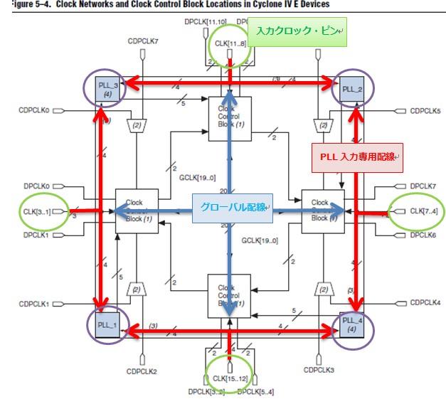
Figure 1. Cyclone® IV E global routing architecture
Cyclone IV E has PLL_1~4 on the four corners of the device. It is implemented on the global routing by pin assignment to the input clock pin (= CLK [*] ). Pin out the signal that drives the PLL to CLK [*].
Place and route to optimize PLL phase alignment
Even if the signal driving the PLL is pinned to CLK[*], there are cases where the routing used does not compensate for the phase alignment characteristic of the PLL. The Fitter issues a Critical Warning (Figure 2) when a wire that is not phase-compensated is used.
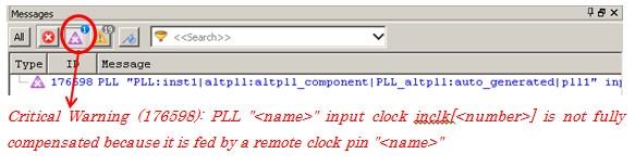
Figure 2. Critical Warning with Uncompensated Phase Adjustment
The Fitter automatically selects routing from CLK[*] depending on CLK[*] placement and PLL/routing region utilization. Therefore, the wiring cannot be specified by the user. You can check the routing results in the PLL Summary (Figure 3) in the compilation report.
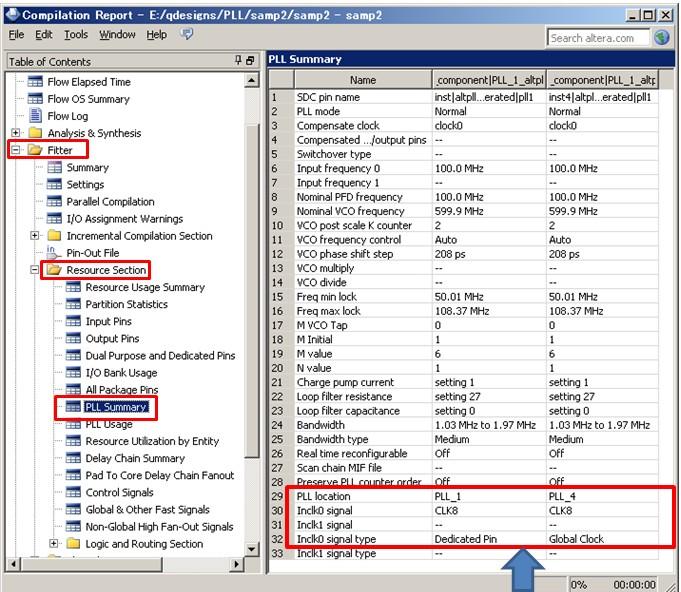
Figure 3. PLL Summary Compilation Report
PLL_1, labeled "Dedicated Pin" in the PLL Summary in Figure 3, has optimized phase adjustment (Figure 4). On the other hand, PLL_4 labeled "Global Clock" is not phase adjusted compensated (Figure 5).
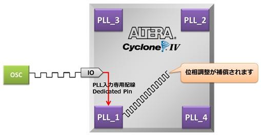
Figure 4. Image of wiring with PLL phase adjustment compensated
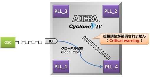
Figure 5. Image of wiring without PLL phase adjustment compensation
Wiring is not user-specifiable. However, by devising the "design" and "pin arrangement", it is possible to guide the Fitter to the wiring where the PLL phase adjustment is compensated (= Dedicated Pin).
| Summary |
|---|
|
Next time, I will introduce how to guide the Fitter to the Dedicated Pin wiring.