- Semiconductor BusinessHOME
- Products and Services of Macnica,Inc.
-
technical information

-
Events and Seminars
- Handling Manufacturer
- Support
- Inquiry
- Click here to purchase products
- Semiconductor business e-mail magazine registration
![]()
![]() Narrow down by specifying conditions
Narrow down by specifying conditions
現在2183件がヒットしています。check


Hello. This is Topuu!
This time, I'd like to summarize the timing analysis, which was the most difficult thing for me to understand throughout the year.
This article is a must-read for FPGA beginners.
About a year ago, I received training on timing constraints, which allowed me to learn about the concept of timing constraints.
However, when it comes to actually designing a circuit and applying timing constraints, it's hard to know where to start.
Questions arose such as, "Is this constraint correct?", and I developed an aversion to timing.
It was my senior colleague who prescribed the medication for me when I was suffering from allergies at that time.
This time, I will explain the advice (constraint procedure) I received from a senior colleague that helped me overcome my difficulty with timing.
First, we need to confirm the timing constraints and the analysis flow (Figure 1).
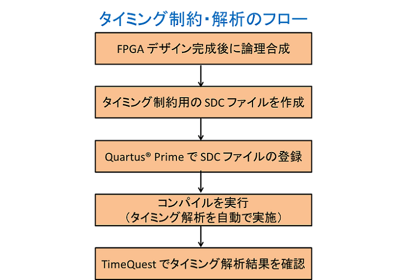
Figure 1. Timing constraints and analysis flow.
This section will explain the procedure for creating the SDC file, which is the first hurdle in this process.
SDC constraints must be applied to all paths in the circuit.
It might seem difficult to apply constraints to every path, but there's a specific order in which to apply the constraints, and by following that order, it becomes much easier!
Figure 2 summarizes the order.
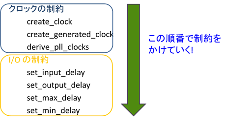
Figure 2. Order of description in the SDC file
Figure 2 shows that there are only two main types of commands required to implement constraints.
For more information on timing constraint commands, please refer to this article.
Since I/O constraints are based on the clock frequency, we'll start by setting clock constraints.
Now, let's immediately apply constraints to the example circuit. We will apply constraints to a circuit as shown in Figure 3.
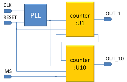
Figure 3. Example of a circuit diagram
`counter: U1` counts up and down for the ones place, and `counter: U10` counts up and down for the tens place.
MS is an external signal used to choose whether to increment or decrement the counter.
In this circuit, there are two paths that impose "clock constraints": the "input clock: CLK" and the "PLL output clock".
First, let's address the constraints on the input clock.
This uses the `create_clocks` command.
If an SDC file does not exist, a new one will be created.
You can create a new SDC file by clicking File → New → Synopsys Design Constraints File.
This time we will be using a 50MHz clock, so we will define a clock with a frequency of 50MHz.
Commands can be easily generated using a GUI.
Right-click where you want to enter the command in the SDC file, then click Insert Constraint → Create Clocks to bring up the GUI. (Figures 4 and 5)
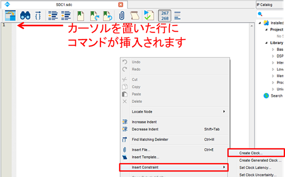
Figure 4. How to access the GUI for generating SDC constraint commands.
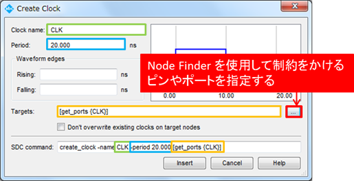
Figure 5. GUI User Screen
Clock name: The name of the clock that imposes the constraint.
It's not necessary to match the clock name in the design.
*The clock name specified here is only valid within the SDC file (for clarity, we've used "CLK," the same as in the design).
Period: Setting the clock period.
Since the clock is 50MHz, we input a period of 20ns.
Targets: Define the ports and pins that will impose restrictions.
Finally, we select the target, using something called `get_port`.
This can be used to search for a port name within the design, and then, using get_port {CLK}, a constraint called create_clock is applied to the port named CLK.
Set the constraints you want to apply, and then click Insert to insert the command into the SDC file. (Figure 6)
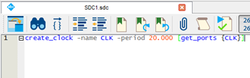
Figure 6. SDC after command insertion
Next, we will set constraints on the PLL output clock.
Enter the derive_pll_clocks command here.
Entering this command completes the constraint on the PLL output clock.
This completes the clock constraints, resulting in the configuration shown in Figure 7.
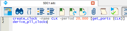
Figure 7. Clock constraints
By imposing the above constraints, we have created a restriction on the part of the circuit shown by the red line in the example circuit (Figure 8).
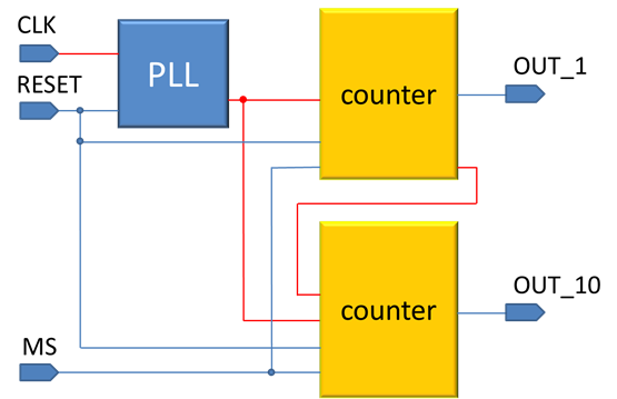
Figure 8. Circuit diagram after constraints have been applied.
Applying a clock constraint imposes a constraint on the path within the circuit region (clock domain) driven by that clock.
I had thought that I had to impose constraints on every single pass, so when I learned this, my internal barrier to timing constraints was lowered. (Figure 9 illustrates this.)
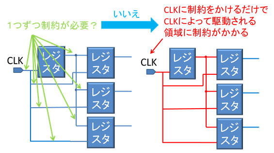
Figure 9. Schematic diagram of a path subject to clock constraints.
Continuing in this manner, I entered timing constraint commands for the I/O section and false paths, and by applying constraints in this way, I felt that I was able to apply constraints more smoothly than before, when I had a hard time with it.
For more information on I/O constraints, please see this article!
bonus
In this instance, we defined the PLL output clock using the derive_pll_clocks command,
If there are multiple PLL output clocks, there is a command to impose constraints on each one individually.
That's the create_generated_clock command.
Using Figure 10 as an example, the same constraints were applied using the create_generated_clock command and the derive_pll_clocks command, respectively.
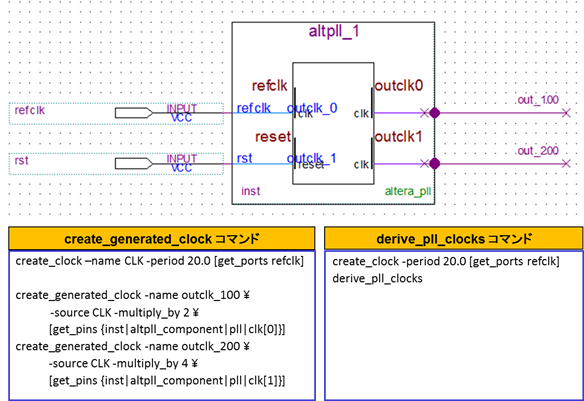
The `derive_pll_clocks` command is much simpler to use!
The `create_generated_clock` command allows you to impose constraints on each individual output clock, making it useful when you want to modify the clock shift amount or perform timing verification.
(Using derive_pll_clocks would require starting over with design modifications.)