
![]()
![]() Narrow down by specifying conditions
Narrow down by specifying conditions
現在1888件がヒットしています。check
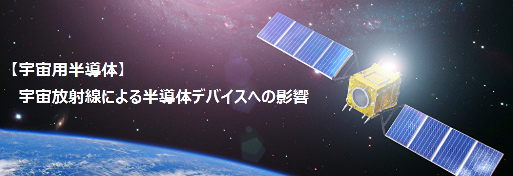
Harsh Space Environment for Semiconductor Devices
As you know, outer space is full of high-energy radiation.
When semiconductor devices are used in outer space, the environment is different from that on Earth. special test clear the radiation tolerant semiconductor devices As
Approved parts must be used.
This time, we will explain the "effects on semiconductors of concern in harsh space" for semiconductor devices.
Effects on semiconductor devices in the space environment
When using semiconductor devices in outer space, it is necessary to consider the effects of cosmic radiation.
In outer space, radiation such as X-rays and gamma rays electromagnetic waves and consists of particle beams such as protons, electrons, and heavy particles radiation has become an environment where
On the ground, the direct effects of cosmic radiation are small thanks to the atmosphere and geomagnetism, but in outer space, we are directly exposed to cosmic radiation.
The impact is great, and in the past it was said that "semiconductor devices mounted on artificial satellites Failure due to radiation effects There are also cases where
Next, I will explain the effects of the space radiation environment on semiconductor devices.
Space radiation environment that greatly affects semiconductor devices
In outer space, there are three types of space radiation environments that have a significant impact on semiconductor devices.
- A solar flare consisting mainly of protons coming from the Sun
- The Van Allen belts, which are mainly composed of protons and electrons, captured by the Earth's geomagnetic field.
- Galactic cosmic rays composed of high-energy heavy particles from outside the solar system due to supernova explosions, etc.
What are the effects of cosmic radiation in these three environments on semiconductor devices?
When cosmic radiation enters a semiconductor device, it generates electric charges due to its ionization effect.
The charges generated here cause the following phenomena that adversely affect semiconductors.
Due to these phenomena, of semiconductor devices "Characteristics deterioration or malfunction, damage] and other adverse effects are caused.
During the mission period of artificial satellites, etc., "What is the probability of occurrence?"
etc., in advance, need to take action there is.
So far, Adverse effects of the cosmic radiation environment on semiconductor devices and possible consequences"Characteristic deterioration or malfunction, Damage” and
themeasures are very important Did you understand what was going on?
In the next and subsequent articles, we will talk about the phenomena "SEE" and "TID" that cause such problems, and "If a problem occurs,
What will happen? I will delve into and explain about. looking forward to.
If you have any questions about radiation, please consult Macnica!
Macnica also accepts inquiries regarding "up-screening" and "radiation resistance testing/evaluation (TID / SEE) requests".
In addition to consulting on radiation testing, we also provide support for the following "reliability of space semiconductor devices".
- Implementation support for tests, inspections, and analyzes at external facilities in Japan and overseas, and interface with facilities
- Conducting non-destructive testing using Macnica 's in-house X-ray inspection equipment
If you have any problems regarding “space semiconductors,” please feel free to contact us using the inquiry form below.
We will provide support based on Macnica 's "rich experience" and "high technology."