![]()
![]() Narrow down by specifying conditions
Narrow down by specifying conditions
現在1889件がヒットしています。check

This is Sasaki in charge of power supply dock technology.
In this column, I would like to introduce some examples of problems related to power supplies that I encountered multiple times during various customer support sessions.
A customer asked us a question via the contact form.
多電源・低電圧化による現象

Recent devices, not limited to FPGA, require multiple power supplies and are really difficult to design.

What are the difficulties?
First of all, the demand for low voltage and high current is increasing, and precision is required more and more.
I agree. As mentioned in the 14th column, wiring resistance and 0 (zero) Ω resistance on the board can also cause problems.
Yes, there are other more demanding power sequencing requirements.
It is true that when a variety of devices are mounted on a board, it is difficult to perform sequence control using the time constants of resistors and capacitors as in the past, and a microcomputer or sequencer must be used.
That's right.
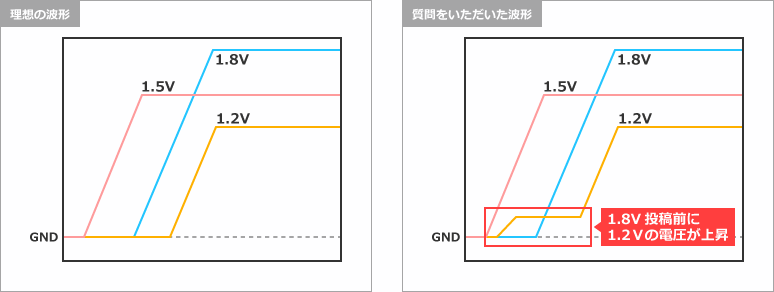
So, what I would like to ask you this time is that voltage leaks out from the I/O pins of devices such as microcomputers and FPGAs, even though you should have followed the power sequence required by the device to turn on the power.
As a result, the requested power sequence cannot be observed (see the figure below).
So that's it. You don't need to worry about this.
When I monitor the voltage, it looks like the sequence is not kept, but the sequence of the externally supplied power satisfies the device's requirements.
e? ! Really?
Yes, what the device requires is the regulation of the supplied voltage sequence, and the leaked voltage from the device's I/O etc. can be ignored.
Really! Good then.
So why is voltage leaking out from things like I/O? Are there any issues with the quality of the device?
Since the logic inside the device is not fixed until all the power supplies are turned on, the inside of the device is a mass of resistors and diodes made of PN junctions.
As a result, the I/O may see voltage through a junction with low resistance.
There is no quality problem, so please use it without worry.
I see.
The point of this time
As long as you follow the power sequence, you don't have to worry about leakage voltage from the I/O pins.
Introduction of opinions sent to the question form
[question 1]
There is no problem with the FPGA, but I think that the voltage is applied to the output terminal of the power supply when the input voltage of the power supply that supplies 1.2V is zero. Is there any problem with this?
[Answer]
We believe that there will be no problem in terms of power if the leakage current or voltage is applied from the FPGA side.
The reason is that the resistance value of FPGA is several KΩ or more, and the current value is limited to mA order or less.
Therefore, the FET on the DC/DC side will not be damaged and will not be a problem.
[Question 2]
Is it possible to apply voltage to the output side of any DC/DC converter when the input voltage is zero?
[Answer]
Intentional application of voltage is NG, but there is no problem as long as the potential rise due to leakage current of FPGA, CPU, etc. is applied.
An example of a problem is when a large capacitor is connected to the output of a DC/DC when there is no voltage.
In this case, a large charge remains in the capacitor, which may flow back to the DC/DC side and damage the FET on the low side of the DC/DC.
Click here for recommended articles/materials
Click here for recommended seminars/workshops
Analog solution power supply design seminar
Analog solution thermal design seminar
Basic seminar on power supplies for digital circuit designers