![]()
![]() Narrow down by specifying conditions
Narrow down by specifying conditions
現在1888件がヒットしています。check

This is Sasaki in charge of power supply dock technology.
In this column, I would like to introduce some examples of problems related to power supplies that I encountered multiple times during various customer support sessions.
A customer asked us, ``During a comparative evaluation of the DC/DC converters of Company A and Company B, we encountered a problem where the power supply IC burned out, so we would like support.''
評価方法は十分に注意
詳しい症状はこちら
- A 社と B 社の電源 IC はピンコンパチ品
- 過去に A 社で設計した基板を使用した試作評価中に焼損が発生
- A 社の電源 IC を使用した場合、焼損は起こらない
- B 社の電源 IC を使用した場合のみ、焼損が発生する

評価ボードで検証していた時は、B 社の電源 IC も全く問題無かったのですが、自社の基板で評価を始めたら焼損が発生するようになってしましました。
価格面ではB社が魅力的なので、ぜひ使いたいのですが・・・

そうなんですね。ではまず、回路図とレイアウト図を確認させていただきますね。
回路図とレイアウト図を確認
回路図も B 社の電源 IC 用に定数変更していますし、レイアウトも問題なさそうですね。
なにが原因なのでしょう・・・
全く動かない状態ですか?
いいえ、はじめは正常動作しているのですが、評価途中で焼損してしまいます。
では、実際に評価しているところを見せていただけますか?
実験室へ移動し、実際に評価方法を見てみると、、、
(なるほど。そういうことだったのか!)
原因が分かりましたよ。
どうやら評価方法に問題があったようです。
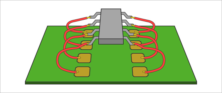
電源 IC を基板に実装せず、リード線で基板と接続しているせいで焼損が発生しています。
え!電源 IC の変更が楽なのでリード線で接続して評価していたのですが、これだとダメなんですか?
この方法だと、GND 接続部のリード線のインダクタンス成分によって電源ICの絶対最大定格を超える電圧が発生し、電源 IC が焼損する可能性があるんです。
そうなんですね。。。では電源 IC を基板に実装して評価をしてみます!
After that, when we mounted the power supply IC on the board and performed the same evaluation, no burnout occurred.
電源 IC が焼損した原因
電源 IC を基板に実装せず、リード線で接続していたこと。
The point of this time
When evaluating power supply ICs, be sure to mount them on the board!
(If you don't take the time to do this, it will cause problems like this one.)
Click here for recommended articles/materials
Click here for recommended seminars/workshops
Analog solution power supply design seminar
Analog solution thermal design seminar
Basic seminar on power supplies for digital circuit designers