![]()
![]() Narrow down by specifying conditions
Narrow down by specifying conditions
現在1888件がヒットしています。check
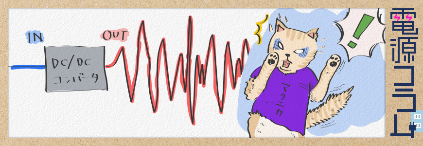
This is Sasaki in charge of power supply dock technology.
In this column, I would like to introduce some examples of problems related to power supplies that I encountered multiple times during various customer support sessions.
ある日、お客様からこんなお問い合わせがありました。
仕様は満足しているはずですが・・・

I am having trouble with the output power becoming unstable when I increase the input voltage of the DC/DC converter. . .
お客様が直面したトラブルの詳細はこちら
- 出力電圧が不安定で、低周波数で変動をしているため、FPGA の電源要求を満たさない
- 入力電圧、出力電圧は規定範囲内
- 周辺回路については回路定数の問題なし
そこで早速お客様先を訪問。
When observing the output voltage and switching waveform of the DC/DC converter with an oscilloscope...
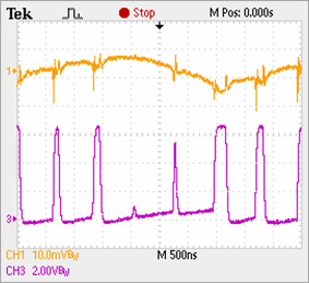

スイッチング波形が崩れています。出力電圧が不安定になった原因はこれですね。
この電源 IC は、今の回路条件で入力電圧を 7V 以上にすると、出力電圧を低くすることができないんです。
え?でもこの製品のデータシートには『28V まで入力可能』と書いてありますよ。
データシートが間違っているということですか?
Switching DC/DC converters have a minimum on time that is determined by the input/output voltage difference and switching frequency.
This time it seems to be in an unstable state because it does not meet the regulations.
出力電圧が不安定になった原因 → Minimum On Time 規定の逸脱
For switching DC/DC converters, the average voltage during on/off switching operation (PWM) is the output voltage. When obtaining a lower output voltage from a higher input voltage, the switching on time is shorter. Minimum On Time is how much you can shorten the on time.
今回はオンの時間を非常に短くしたことで Minimum On Time の規定を逸脱し、出力電圧が不安定になっていました。
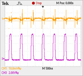
When I tried lowering the input voltage a little (slightly longer switch on time), I was able to get a normal waveform within the Minimum On Time specification.
The point of this time
Switching DC/DC converters also require attention to Minimum On Time!
application note
電源のMinimum On Timeの規定を逸脱した場合について、より詳しく解説しているアプリケーションノートがダウンロードできます。
Click here for recommended articles/materials
Click here for recommended seminars/workshops
Analog solution power supply design seminar
Analog solution thermal design seminar
Basic seminar on power supplies for digital circuit designers