- Semiconductor BusinessHOME
- Products and Services of Macnica,Inc.
-
technical information

-
Events and Seminars
- Handling Manufacturer
- Support
- Inquiry
- Click here to purchase products
- Semiconductor business e-mail magazine registration
![]()
![]() Narrow down by specifying conditions
Narrow down by specifying conditions
現在2189件がヒットしています。check

In applications where noise is important, a linear regulator is used instead of a switching regulator. In such cases, if the potential difference is large or the load current is large, heat generation by the linear regulator becomes an issue.
traditional method
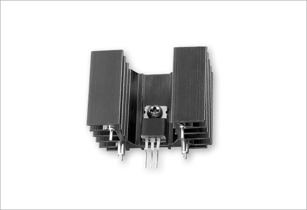
Dissipate heat to a heatsink or housing
When designing for a large housing, we used a linear regulator in a TO-220 package and efficiently dissipated the heat by dissipating it into the housing or by screwing a large heat sink onto it, as shown in Figure 1.
Recently, there has been a need to miniaturize housings and circuit boards, and in cases where a heat sink cannot be used, applications are often designed to reduce power consumption, and QFN packages or similar are used to dissipate heat to the board.
How to reduce fever
Switching regulator and low drop LDO configuration
While it is possible to use a switching regulator on the board, such as for the FPGA core voltage, you may want to have a low-noise power supply for the PLL.
In such cases, heat generation can be reduced by first using a switching regulator to drop the voltage to a low voltage such as 5V or 3.3V, and then using a low-drop LDO as the power supply for the PLL.
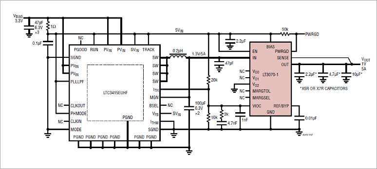
The LT3070-1 from Analog Devices operates normally as a linear regulator as long as the dropout voltage (input-output voltage difference) is 85mV. As shown in Figure 2, it is possible to configure a power supply circuit in which the LTC3415 generates 1.3V in the front stage and the LT3070-1 generates a 1.0V / 5A output.
If you create 1.0V directly from 3.3V, the power loss (Pd) will be 11.5W [(3.3V-1.0V) x 5A].
When converting 1.3V to 1.0V via the LTC3415, the power loss (Pd) is 1.5W, reducing the power loss by 10W and making it possible to suppress heat generation in the LT3070-1.
Configuration using parallel connection of linear regulators
In systems where a switching regulator cannot be used on the same board, a circuit configuration like the LT3070-1 mentioned above cannot be used.
In such cases, you should consider using a parallel configuration of linear regulators.
When connecting in parallel, the problem is how to balance the output current of the linear regulators connected in parallel. One way to balance the output current is to use a "ballast resistor" at the output of the linear regulator. Generally, to improve the balance, the ballast resistor must be made larger, but this has the side effect of worsening the load regulation. This trade-off relationship makes it more difficult to design a parallel connection.
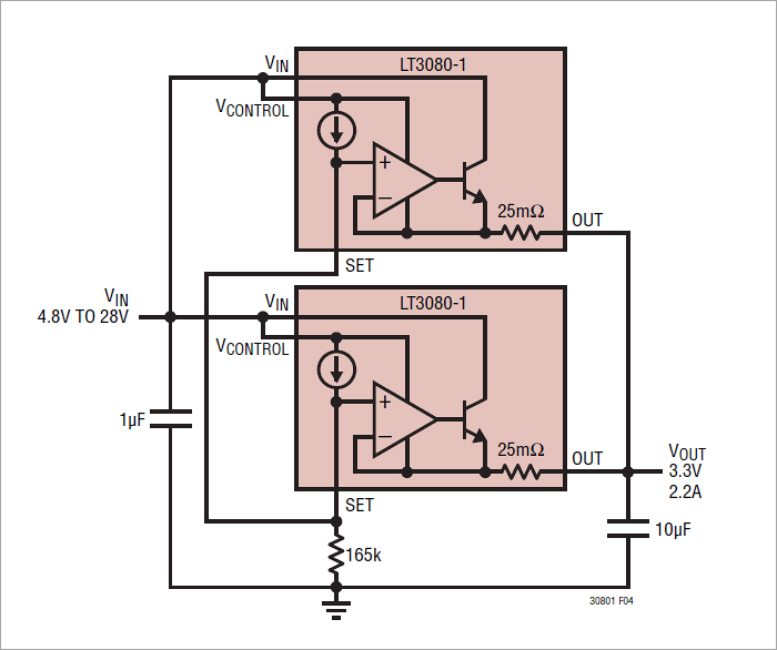
LT3080-1 with integrated ballast resistor
The Analog Devices LT3080-1 is a parallelable linear regulator.
As shown in Figure 3, a 25mΩ ballast resistor is built in to ensure equal current sharing.
In Figure 3, two parallel connections provide a 2A output, but the output current can be increased by increasing the number of parallel connections. Also, if you increase the number of LT3080-1s in parallel from two to four for a circuit that requires a 2A load current, the load current burden per unit will be reduced to 500mA, which will reduce heat generation and make heat dissipation design easier.
This linear regulator is ideal for those who can only use linear regulators and have difficulty with heat dissipation design.
Related Information
Click here for recommended seminars/workshops
Click here for recommended articles/materials
Click here to purchase products
Click here for manufacturer site/other related links
LDO Linear Voltage Regulators Product Information
LT3070-1 Product Information
LT3080-1 Product Information
Inquiry
If you have any questions regarding this article, please contact us below.
Analog Devices Manufacturer Information Top
If you want to go back to Analog Devices Manufacturer Information Top, please click below.