- Semiconductor BusinessHOME
- Products and Services of Macnica,Inc.
-
technical information

-
Events and Seminars
- Handling Manufacturer
- Support
- Inquiry
- Click here to purchase products
- Semiconductor business e-mail magazine registration


 Narrow down by specifying conditions
現在2236件がヒットしています。check

This content aims to organize and deepen designers' understanding of the correct design methods and knowledge for FPGAs and CPLDs, thereby demonstrating that Altera® devices are user-friendly and highly reliable, while simultaneously minimizing unstable elements in the device design.
In FPGA and CPLD development, building a reliable (i.e., functional) system requires learning the fundamentals of key design techniques and implementing them in the device. However, understanding the operating characteristics of FPGAs and CPLDs is also crucial as preliminary knowledge.
The main factors that can prevent FPGAs and CPLDs from functioning correctly are as follows:
- voltage fluctuation
- Ambient temperature
- Lot variation, process evolution
These external factors are very common, and fluctuations in them will also cause fluctuations in the timing (delay) of FPGAs and CPLDs. For example, the higher the voltage and the lower the temperature, the smaller the delay and the faster the operation. Many malfunctions are caused by this variation in timing. We often hear things like, "It worked after I replaced the device," or "It worked after I cooled the device." In most cases, these stem from timing problems. Herein lies a problem that is often overlooked. In the short term, variations between device batches can be considered, and in the long term, changes in delay values due to process evolution can be considered.
On the other hand, the delay values of FPGAs and CPLDs are defined under at least two operating conditions: the fastest operating condition (Fast) and the slowest operating condition (Slow). (FPGAs with a 65nm process or less have three conditions, and FPGAs with a 28nm process or less have four conditions.) The development software has a library (timing model) for each operating condition. Even if the device lot changes or a process change is performed, the device will remain a normal device (good product) as long as it does not violate the specified fastest and worst-case timing models.
If you don't have a good understanding of these things beforehand when designing, you'll run into unexpected problems. No matter how good a device manufacturer claims a product is, it's useless if the system doesn't work. So, let's clarify the concept of a good product (at least in terms of specifications) that a device manufacturer will ship.
production lot
Generally, each device comes in a lineup of several speed grades, such as 6-speed, 7-speed, and 8-speed grades. While each of these speed grades has its own timing model, slower devices may include faster devices. In other words, a speed grade 8 device may also have the performance of a speed grade 7 device. To put it another way, a speed grade 8 device may have the performance of both speed grade 7 and speed grade 8 devices. This ambiguity in FPGA and CPLD design can sometimes lead to malfunctions due to timing variations.
process change
When a process change is implemented, the same timing model as the previous product is used, similar to issues with manufacturing lots. However, the delay value tends to become faster due to the process change. As a result, using a product made with the new process can lead to problems such as "noise causing malfunctions," "glitches occurring," and "counter malfunctions due to ground bounce."
timing model
The operating conditions recommended by Altera® are as follows:
- Operating voltage range (V)
- Ambient operating temperature range (T)
- Lot variation (including process change) (P)
Under these PVT conditions, timing models for development software are provided. When verifying the timing of Altera® FPGAs/CPLDs (timing analysis with TimeQuest or timing simulation with EDA simulator tools), there are two timing models used: the Fast model, which represents the fastest operating conditions, and the Slow model, which represents the slowest operating conditions. However, analyzing all paths of the circuit using only these worst-case values is actually insufficient. Lot variations must also be considered. This is because a device where some parts of the circuit operate slightly faster due to lot variations may have tighter timing requirements than a device where all parts of the circuit operate at the slowest possible speed. This type of analysis is called Minimum/Maximum analysis, and Quartus® Prime performs analysis that takes these factors into account.
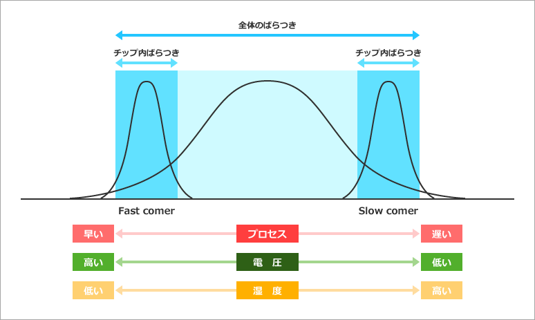
The results calculated by Quartus® Prime are values that meet the user's design requirements in clock-synchronous designs. For example, the operating frequency (Fmax) in the Slow model obtained from TimeQuest indicates the lowest operating frequency of the slowest path of the device, ensuring that the operating frequency of the system used is below that frequency. Similarly, by ensuring the calculated setup/hold time values on the system, it will operate under Altera® 's recommended conditions.
For these reasons, when using Altera® FPGAs or CPLDs, we recommend performing thorough operational verification through timing analysis after compilation is complete (after placement and routing).
The above covers the basic knowledge required for FPGA/CPLD design.
Click here for recommended articles/materials
[A must-see for RTL design beginners] Differences between synchronous and asynchronous design
[Must-see for Beginners in RTL Design] Impact on the System when Inputting Asynchronous Signals