- Semiconductor BusinessHOME
- Products and Services of Macnica,Inc.
-
technical information

-
Events and Seminars
- Handling Manufacturer
- Support
- Inquiry
- Click here to purchase products
- Semiconductor business e-mail magazine registration
![]()
![]() Narrow down by specifying conditions
Narrow down by specifying conditions
There are currently 2168 results.
While major FPGA manufacturers are expanding their lineup of high-end FPGAs, the low-end FPGA family "ForgeFPGA™" announced by Renesas is attracting attention as it is in high demand from applications that require small-scale programmable logic. I am collecting. Therefore, based on the provisional version of the development tool "ForgeFPGA Advanced Hardware Kit" obtained in August 2023, we checked the contents and tried launching the development environment. In this article, we will introduce the product specifications and development tools in advance so that you can start development as soon as it is officially released.
Low-end FPGA What is "ForgeFPGA"?
The ForgeFPGA family is a low-end FPGA for applications requiring less than 5,000 logic gates, low power consumption of less than 20 µA during standby, and 1,000 integrated lookup tables.
Aiming to enable a wide range of users to utilize ForgeFPGA while keeping development costs low, we have created an HDL mode that provides a familiar Verilog environment for users with extensive FPGA development experience, and an HDL mode that can be used even by users with little FPGA development experience. Two types of development tools are provided: ``Macro Cell Mode,'' which uses an easy-to-use development flow based on schematic capture.
Product Specifications
A product with the model number SLG47910 is scheduled to be released from the ForgeFPGA family, and we will introduce the specifications by quoting from the preliminary data sheet (download the PDF file from the Renesas website). Please note that the specifications may change after the official release, and the information is as of September 2023.
■ SLG47910 overview
|
High density logic array |
・Equivalent to 900 4bit LUTs ・1.8K DFF ・5kb of distributed memory |
|
clock |
・Built-in 50MHz/3.41MHz oscillator |
|
power supply |
-VDDIO:1.71V to 3.6V -VDDC:1.1V±10% |
|
package |
-24-pin QFN: 3.0×3.0mm, 0.4mm pitch (19 GPIOs) -20-pin WLCSP: 1.85mm x 1.64mm, 0.35mm pitch (15 GPIOs) |
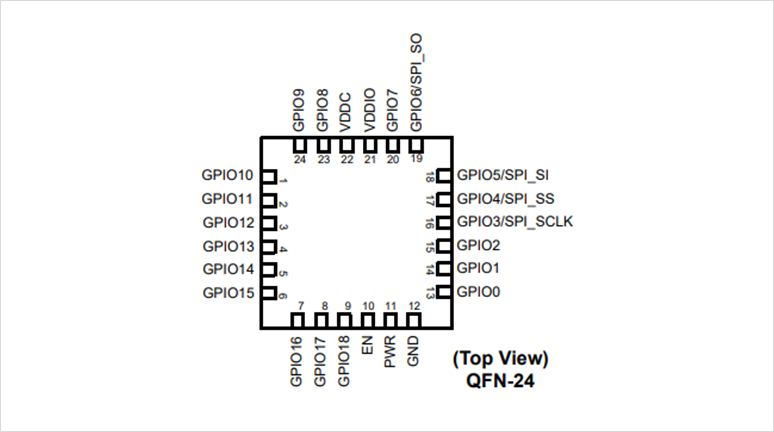
Figure 1. Package 24-pin QFN
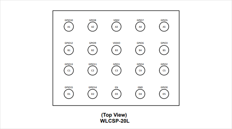
Figure 2. Package 20-pin WLCSP
Internal block diagram
The features understood from the SLG47910 block diagram are as follows.
・Built-in 384KB One Time Program memory (OTP): FPGA connection information and macro cell setting data can be stored in the IC's internal memory.
・Built-in oscillator and configuration memory (Configuration RAM): No external components required, reducing BOM cost
For designers who use FPGAs to build large-scale circuits such as interface conversion around microcontrollers and decoding circuits for orthogonal encoders, BOM costs can be reduced by reducing external components such as external oscillators and configuration memories. This not only reduces the amount of energy used, but also shortens the design and development period.
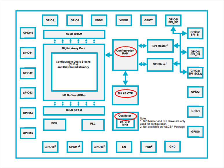
Figure 3. Internal block diagram
opening ceremony
From here, we will explain the ForgeFPGA Advanced Hardware Kit. The contents of the kit I received are as follows.
ForgeFPGA Advanced Hardware Kit includes:
・Power adapter
・Development Board
・Socket Adapter Board
・USB Type-C cable
・SLG47910V IC chips (blank chips) x 25 pieces
Figure 4. ForgeFPGA Advanced Hardware Kit box.
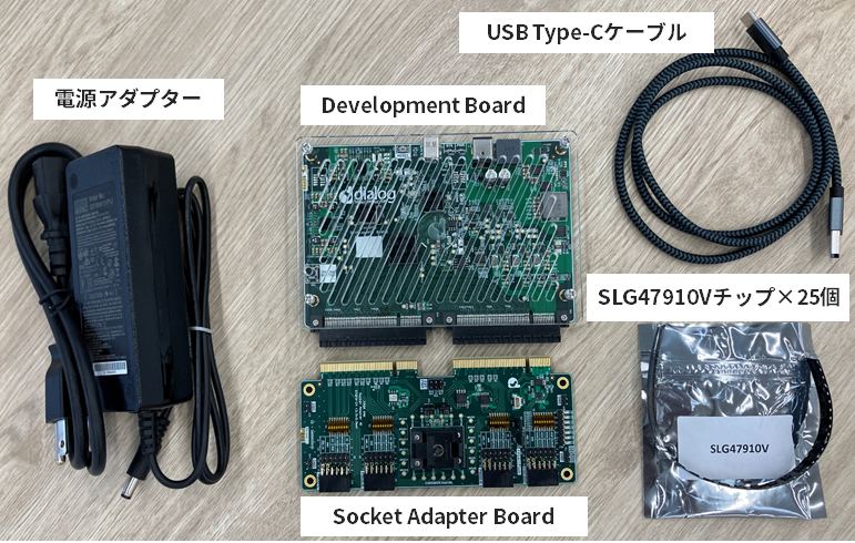
Figure 5. Contents of the ForgeFPGA Advanced Hardware Kit.
Connection with PC
The Development Board has one power adapter terminal and one USB Type-C connector, and connect them as shown below.
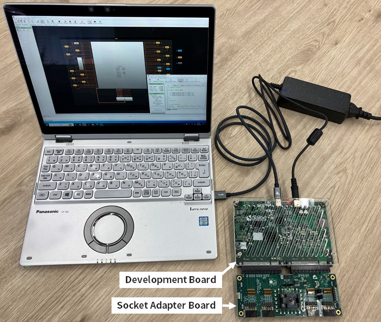
Figure 6. Connection between PC and Development Board
Check the operation!
I wrote an AND circuit using a Verilog-based tool called ForgeFPGA Workshop and tried emulating it.
When I connected the IN1 and IN2 terminals to the VDD_IO terminal, the LED connected to the OUT terminal lit up, confirming that it was working properly.
With the above, we were able to confirm the operation of the ForgeFPGA Advanced Hardware Kit without any problems.
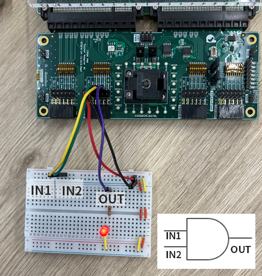
Figure 7. Normal operation (LED lit) confirmed.
Inquiry
If you have any questions or concerns, please contact us below.
the Company product staff will respond.

