- Semiconductor BusinessHOME
- Products and Services of Macnica,Inc.
-
technical information

-
Events and Seminars
- Handling Manufacturer
- Support
- Inquiry
- Click here to purchase products
- Semiconductor business e-mail magazine registration
![]()
![]() Narrow down by specifying conditions
Narrow down by specifying conditions
現在2183件がヒットしています。check

About this blog
I have been working as an FPGA technical support person for Lattice products for nearly 15 years.
I ended up in charge of supporting the AI solution that Lattice suddenly announced.
Of course, I have no experience working with AI so far, and I am studying from scratch in order to somehow manage my work. I can't quite get from 0 to 1...
In this blog, I will share the process of implementing AI functions on FPGA, and hope that it will serve as a guide for those who are considering it in the future.
Is embedded AI development really possible?

Lattice's AI solution seems to use the mechanism of deep learning among AI,
What is this for an AI beginner like me? That's what it feels like.
Although I was suddenly asked to provide support for AI solutions, I myself had various concerns.
First point.
Normally, when we think of AI, we imagine it using high-spec CPUs and GPUs to perform extremely difficult arithmetic processing while consuming a lot of power.
On the other hand, in the embedded world, there are many cases where various resources are extremely limited, including power.
Is it really possible to use AI in the embedded world? I have a concern.
As for the second point,
If you google about AI development, you will usually find things that seem to be difficult to code in Python language using Linux OS.
Like Tensorflow or numpy... And you may need to customize it according to what you want to do.
I was worried that such a thing would not be possible without asking a design company that specializes in AI.
By the way, I can read Verilog and C language to some extent, but I do not understand Python very well.
I also have a little experience with Linux development.
As a third point,
In order to use the mechanism of deep learning, it seems that training (learning) of the neural network model is necessary.
It seems that the neural network model (NN model for short) makes various decisions like the human brain.
In order to improve the performance of this NN model, it seems necessary to prepare learning data called teacher data and give it to the NN model for learning.
However, in the case of image recognition, for example, the training image data to be prepared seems to be on the level of thousands or tens of thousands, and it is impossible to prepare such data by yourself!
I could go on and on about other things, but I wonder if embedded AI development is really possible... Don't worry.
I am such a person, but this time I actually tried to incorporate processing that detects the upper body of a person and surrounds it with a green frame as shown below.
I would like to describe the process.
It looks like there are some reference designs out there.
It seems unlikely that I will be able to develop everything myself from scratch, so I will first look for a design that will serve as the basis for development.
In providing the solution, Lattice provided a free reference design, so I decided to check the details.
If you go to Lattice's site, it certainly seems that various AI reference designs are provided.

I would like to consider the implementation using this reference design.
As a subject, I decided to use a reference design for Object Counting (counting the number of people).
Using an evaluation board called Lattice's Voice & Vision Machine Learning Board (VVML Board for short),
I would like to implement the object detection (human detection) function on the FPGA called CrossLink-NX.
Click here for details of the FPGA used

This evaluation board (VVML Board) is equipped with a Himax image sensor (HM0360) and is connected to the FPGA.
Using the video data input in real time from this sensor, the FPGA uses AI processing to determine whether or not a person is in the image.
It is in the form of processing up to the point of drawing a square frame around the detected person.
I checked the human detection operation
I'd like to move on, but when I looked at the user guide for the reference design, it's 78 pages long...
CrossLink-NX Object Counting Reference Design User Guide
CrossLink-NX Object Counting Reference Design Project File
My heart was about to break from the beginning,
I found that there is not only a reference design, but also a ready-made demo file.
It's hard to look at the reference design in detail all at once, so using the demo file of this reference design,
I would like to see the final behavior first to motivate the implementation. (Note: Of course the demo file is also free)

Check the demo as shown in the figure below. Write the provided file to the evaluation board,
After that, you can check it very easily because you just look at the image with a free capture tool.
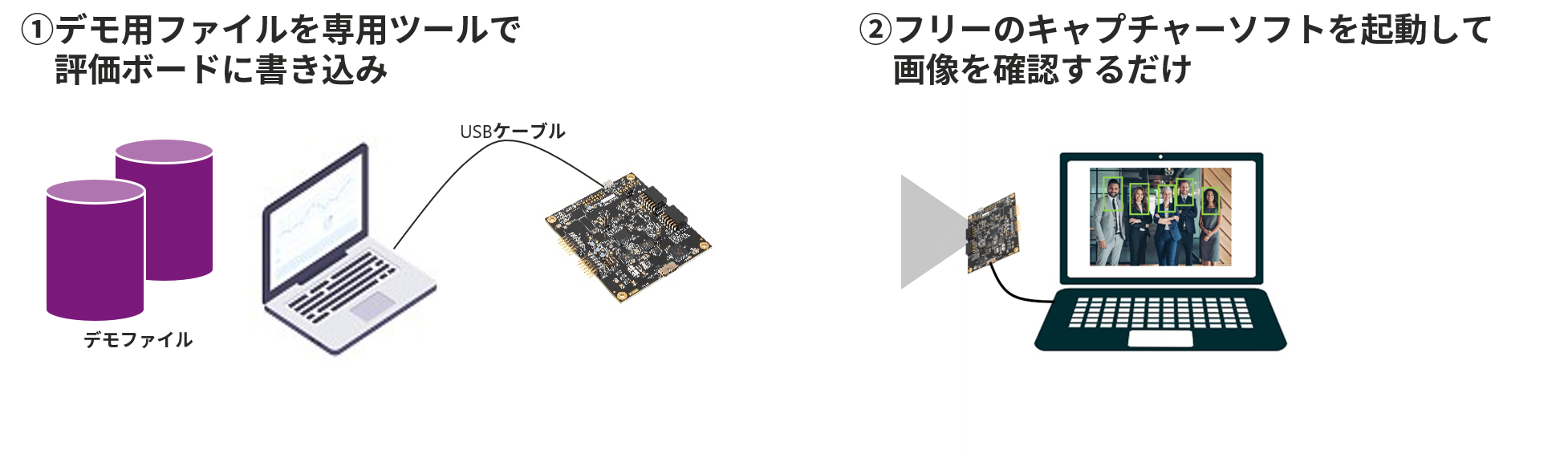
1. Download demo files
I just downloaded the demo file.
The demo file is distributed in zip file format, and when I answered zip,
・ FPGA configuration file generated using Lattice's FPGA design tool "Radiant"
(CrossLink-NX-Human-Counting-Bitstream.bit)
・ A file containing the contents of the AI neural network model
(crosslink-mv2-dual-core-8k.mcs)
included two of
2. Write the demo file to the board
A demo user guide was also provided.
It seems that you can check the operation of the demo by writing these two files to the SPI Flash on the VVML Board using the writing tool "Radiant Programmer" that comes with Radiant.
Click here for demo user guide
FPGA programming tool Programming tool "Radiant Programmer" is here
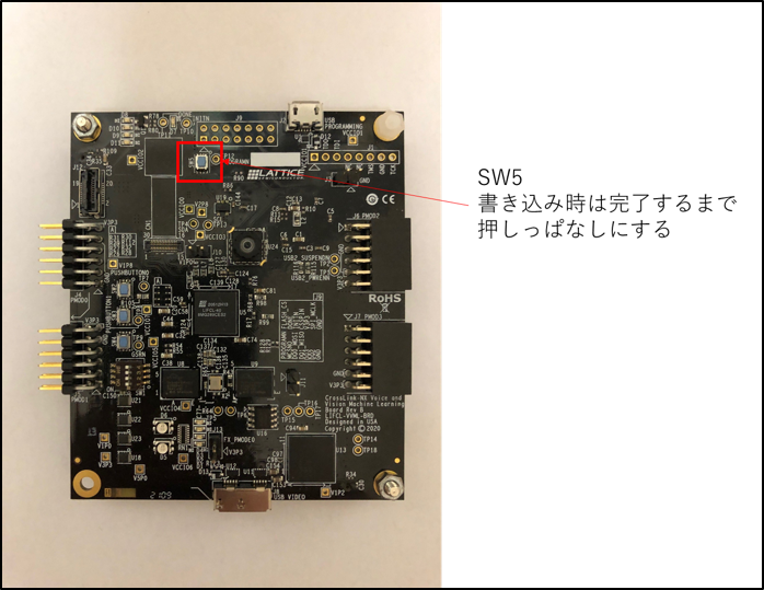
Connect VVML Board and PC with micro USB Type-B cable.
The VVML Board has two USB connectors, a micro USB Type-B connector (J2) and a larger micro USB Type-B SuperSpeed connector (J8).
J2 is used for writing. When the cable is connected, power is supplied from the PC to the board.

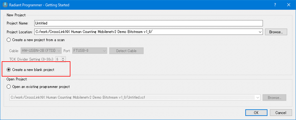
Launch Radiant Programmer from Windows Start.

Select "Create a new blank project" and press OK
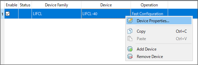
When the Programmer main screen starts, select "LIFCL" (=FPGA model number) from the Device Family column.

The VVML Board is equipped with a CrossLink-NX 40k Logic Cell device, so select "LIFCL-40" from the Device column.

Erase the SRAM area of the FPGA once before writing.
Right-click and select Device Properties to open the Device Properties window.
To erase the SRAM area, set as follows and click OK.
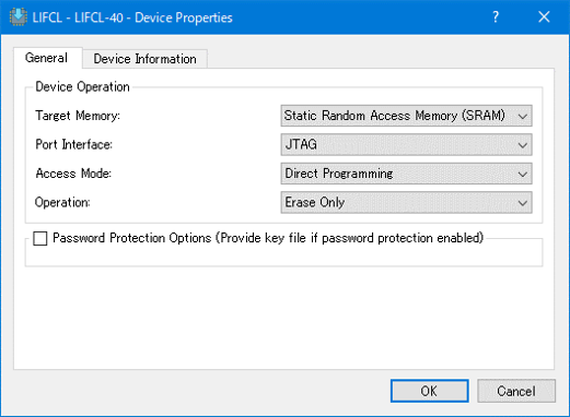
Press the Program button on the toolbar to execute Erase.

When Erase is completed, "Operation: successful" is displayed in the log window at the bottom of the screen.

Next, write the configuration data and network model files.
Write each to the specified address, but first write the FPGA configuration data (CrossLink-NX-Human-Counting-Bitstream.bit).
Similarly, open the Device Properties window and make the settings as shown below.
FPGA configuration data is written to addresses 0x00000000 to 0x00100000.

Click the "Program" button on the toolbar to write.
At this time, as a note, before clicking the Program button, click the Program button while pressing the switch SW5 on the board,
It is necessary to keep pressing SW5 until the writing is finished.
(There was also a description to that effect in the demo's user guide)
After writing the configuration data,
Similarly, write the network model data (crosslink-mv2-dual-core-8k.mcs) to addresses 0x00300000 to 0x00400000.
It is necessary to press SW5 at this time as well.

3. Execution of the demo "Human detected!"
When both data writing is completed, remove the micro USB cable once,
Next, connect the micro USB Type-B SuperSpeed connector (J8) to the computer.
The image output from the FPGA is sent to the PC via USB via the USB microcomputer (Cypress FX3) on the board.
Check this image with a capture tool.
After connecting with the cable, the FX3 is recognized as a camera in the Windows device manager.

I will use AMCAP as a free capture tool. (*It seems that the camera app that comes with Window 10 can also be used as a substitute.)
Click here for AMCAP download link
After installing AMCAP and starting the tool, you can check the demo operation by selecting FX3 from the Devices menu.

The area around the human face is tracked with a green square frame, and the number of detected people is displayed numerically at the bottom left of the screen.
As I showed you at the beginning of the article, you can track at a fairly fast speed! It's pretty interesting.
I checked the power consumption.
Lattice's AI solutions are extremely low power and small,
It claims to be the best AI solution for edge computing.
This AI solution has actually been adopted in notebook computers overseas, where it can detect the presence or absence of people to improve battery usage efficiency,
For security purposes, it is used as a feature to detect people looking in from behind the user.
It means that it is a low power consumption solution that can be implemented in a notebook computer.
By the way, in the case of this design, I would like to measure how much power it consumes.
However, I wanted to actually measure the power using the evaluation board, so I checked the circuit diagram and so on.
Unfortunately, it was a bit difficult to measure directly, so
Using the power consumption estimation tool "Power Calculator" attached to Lattice's FPGA design tool "Radiant",
I tried to estimate the power consumption of the design to be implemented.
After reading the reference design project with Radiant, execute up to placement and routing,
Start the Power Calculator and check the estimated power consumption for each power line.
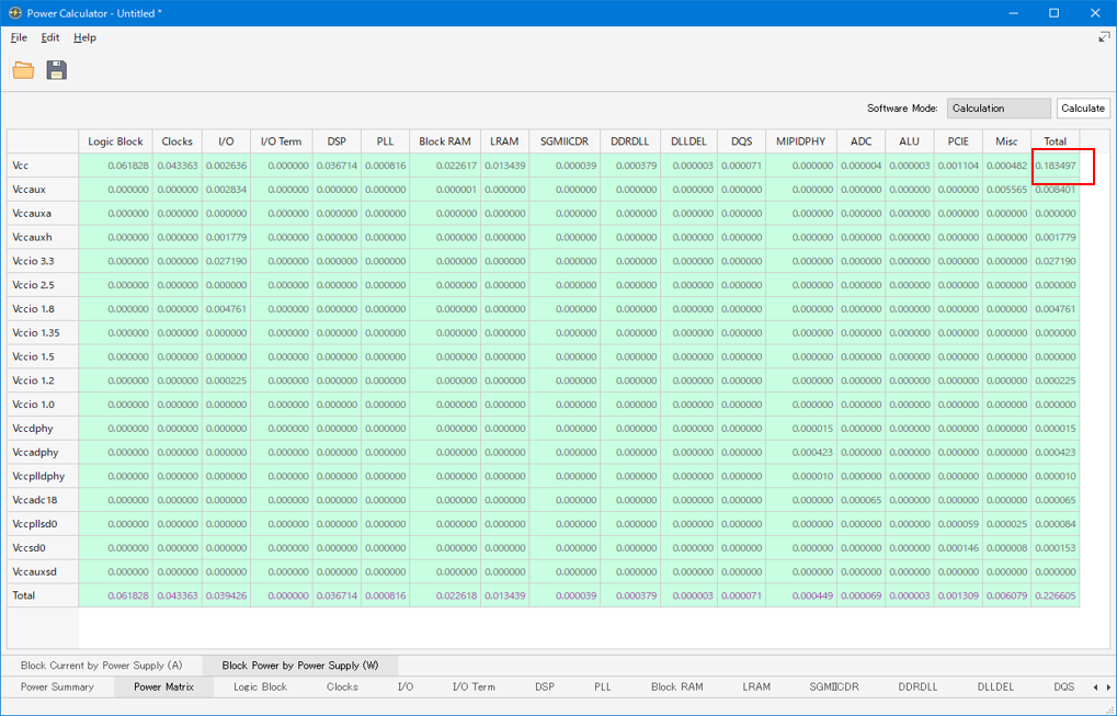
Looking at the CrossLink-NX core power supply (VCC)...
About 200mW!
The total power consumption is about 230mW. (Estimated at ambient temperature of 25°C and AF rate of 20%)
The power consumption is similar to single board microcontrollers such as Raspberry Pi Pico and Arduino Nano.

From Lattice, this design uses 224x224 pixel images for AI processing.
It is announced that processing can be done at a speed of about 10 frames per second.
When considering a single board microcomputer with about the same power,
So far, I have never heard of anything that can perform AI processing using images at this speed.
In addition, if you look at other CrossLink-NX reference designs on the Lattice site,
There are also announcements that even larger images such as QVGA and VGA can be processed even faster.
It certainly seems like a very interesting and edgy solution.
I think that it is a solution that corresponds to "endpoint AI", which indicates the edge side field even among edge AI.
There are signs that it can be used in battery-powered mobile products and IoT-related products.
I would like to make good use of this.
From the next time, I would like to take a closer look at how to proceed with development.
Inquiry
Please feel free to contact us if you have any questions about the evaluation board or sample design, or if there is anything you would like us to cover in this blog!