- Semiconductor BusinessHOME
- Products and Services of Macnica,Inc.
-
technical information

-
Events and Seminars
- Handling Manufacturer
- Support
- Inquiry
- Click here to purchase products
- Semiconductor business e-mail magazine registration
![]()
![]() Narrow down by specifying conditions
Narrow down by specifying conditions
現在2168件がヒットしています。check

The main cause of destroying a device is applying a voltage outside the device's specified range.
From the point of view of the reliability of systems shipped to the market, it is important to take measures such as using protective devices on circuits to prevent device destruction due to overvoltage.
To prevent damage caused by static electricity
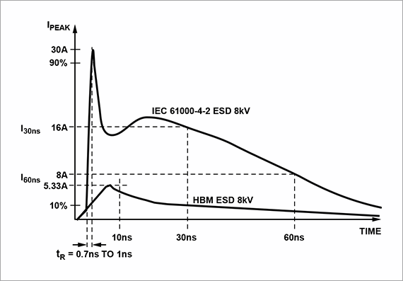
ESD destruction due to static electricity is considered to be one type of overvoltage destruction.
In the case of static electricity, a very high voltage is applied for a short period of time (less than 1 ns), so an ESD suppressor/TVS diode is required as a protective element for ESD protection. For example, you can use an ESD protection element from Würth Electronics (available for purchase here).
Since interface-related parts are exposed to the outside of the housing as metal, ESD countermeasures are particularly important. Analog Devices has developed interface products with enhanced ESD countermeasures, including some that are compliant with the IEC 61000-4-2 Level 3 standard.
For more information, see the ADM3065E, an ESD-enhanced RS485 device.
Overvoltage breakdown due to noise
Noise-induced overvoltage breakdown occurs when noise from the power source or noise generated between devices or boards propagates through power lines or communication lines, destroying devices.
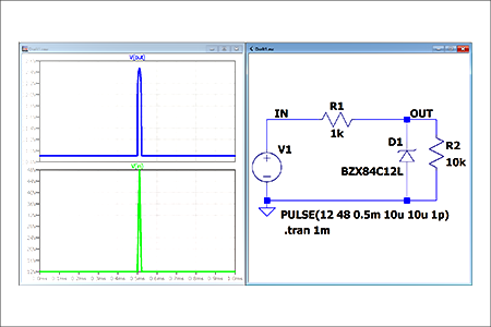
Overvoltage noise can occur when a switch is turned on and off, or when a board or cable is inserted or removed while the circuit board is hot. To counter this overvoltage noise, the breakdown voltage of a Zener diode is used to clamp the overvoltage. Click here for ON Semiconductor's Zener diodes.
The figure on the right shows the results of a simulation using LTspice of the clamping characteristics when a 48V overvoltage noise is applied to an ON Semiconductor Zener diode (BZX84C12L). The figure below shows that an overvoltage of 48V is being input at the input. The figure above shows the simulation results of the 48V overvoltage noise being clamped by the Zener to 12.5V.
Overvoltage generation due to inductive loads and inductance
In systems where the power supply must be connected via a long cable, the inductance of the cable may cause an overvoltage of 1 msec or more when the power is turned on.
Under these conditions, the Zener diode used for noise suppression may consume more power than expected and exceed the allowable power. In such cases, it is necessary to provide a stable power supply to the circuit by inserting a high-voltage power supply IC or module between the power supply and the circuit.
However, power supply ICs and modules require a regulation function to output a stable voltage, so there is a limit to the operating voltage range they can support. Applications that meet these conditions include cameras and sensor modules made for industrial equipment, and automotive equipment.
Overvoltage Protection Solution "Surge Stopper"
As a countermeasure in cases where overvoltage lasting 1 msec or more occurs and protection using TVS or Zener diodes is difficult, surge stopper products developed by Analog Devices can be used.
Before getting into the details of the "Surge Stopper" product, I looked up the word "surge." I discovered that it means "swell" or "big wave." I had some idea that surges mean static electricity or noise, and wondered why it was an overvoltage lasting 1 msec or more, but if it does mean "swell," then it made sense that it was a solution to stop overvoltages lasting 1 msec or more.
The MIL standard (MIL-STD-1275D) specifies the following. We can see that it is required to handle an overvoltage of 500 ms as a surge.
| specification | Normal operating mode | Generator only mode |
|---|---|---|
| steady state | 25V < VIN < 30V | 23V < VIN < 33V |
| spike | up to 250V Energy = 15mJ |
Same as normal operating mode |
| surge | Maximum 40V, about 500ms, RSOURCE = 20mΩ |
Max 100V, about 500ms, RSOURCE = 500mΩ |
| ripple | Magnitude ±2V | magnitude ±7V |
MIL-STANDARD PROVISIONS (MIL-STD-1275D)
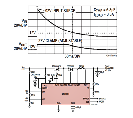
The figure on the right shows the circuit diagram of the surge stopper product LTC4364 and the waveform when a 92V surge is applied.
If a surge voltage is input to the 12V line, the LTC4364 controls the FET (FDB33N25) to clamp the voltage to the voltage set by the voltage divider resistor. In the waveform on the right, the surge voltage of 92V is clamped to 27V. If the input falls below the clamp setting voltage of 27V, the output will drop in line with the input.
Now, please take a look at the detailed explanation and demonstration video of Surge Stopper products.
Surge Stopper product explanation and demonstration video (video length: approx. 7 minutes)
Click here for recommended articles/materials
Click here for recommended seminars/workshops
Inquiry
If you have any questions about Analog Devices products, please contact us here.
Analog Devices Manufacturer Information Top
To return to the Analog Devices manufacturer information top page, please click below.