- Semiconductor BusinessHOME
- Products and Services of Macnica,Inc.
-
technical information

-
Events and Seminars
- Handling Manufacturer
- Support
- Inquiry
- Click here to purchase products
- Semiconductor business e-mail magazine registration
![]()
![]() Narrow down by specifying conditions
Narrow down by specifying conditions
現在2169件がヒットしています。check
Hello, I'm Hiroki, an engineer (FAE) for Analog Devices (ADI) products at macnica.
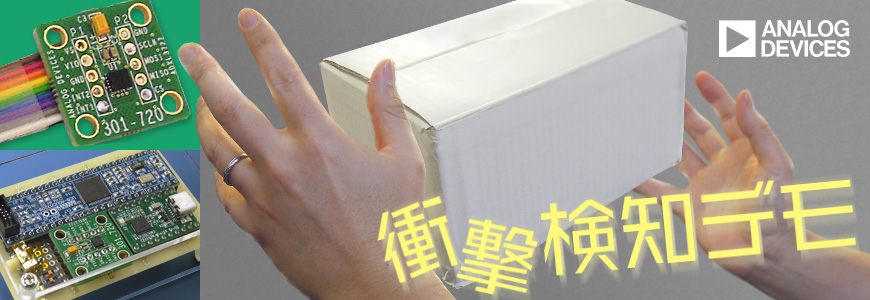
This time, we will introduce the process from conception to completion of a shock detection demo that runs on a single coin battery.
About 5 months, sewing between regular duties. There were nights when I cried because I couldn't check the operation well, but the completed demo attracted a lot of people's interest.
See also here for an image of the shock detection demo.
[Accelerometer ADXL372] Detects shock and vibration during transportation
It's a long post, but there are keywords that are essential for IoT technology, so please keep reading until the end!
- Examination of impact detection demo
- Started building shock detection demo
- [Phase 1] First, verify using ADXL362
- [Phase 2] Verification using production sensor ADXL372
- Effective use of the internal FIFO of the ADXL372
- [Phase 3] Operation check and further improvement on production demo machine
- [Phase 4] Race Against Time! Final adjustments for completion
- Full picture of shock detection demo
- Analog technology seminar was a great success on the day
Examination of impact detection demo
The impetus for building the shock detection demo was to exhibit at the "Analog Technology Seminar" sponsored by ADI, which is held around September every year.
The theme for 2017 is "IoT," which is a hot topic on the street.
Introducing the "sensing technology" that supports this IoT! So, we started looking into it.
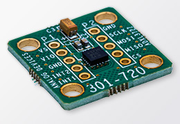
In parallel with normal support work, I used the ADuCM3029 board and the ADXL362 evaluation board (EVAL-ADXL362Z) from Kaneko Systems, an authorized third vendor of ADI, to verify the operation of the ADuCM3029 and ADXL362. During this time, I created a test board (Fig. 1) and "played around" with it. This ended up being the initial prototype board.
In May 2017, the team decided to build a shock detection demo using the ADXL372 based on the initial prototype board. However, even though the basic operation check of the ADuCM3029 (LED blinking, external interrupts, UART communication, etc.) was completed, I was busy with normal work, and the days I couldn't handle continued.
Started building shock detection demo
The 2017 Analog Technology Seminar will be held from September 28th. I started preparing a demo for this.
Senior employee S and I were assigned to build the demo.
H/W development and GUI development during demo ⇒ Mr. S
Application development for ADuCM3029 ⇒ Me
At this point, we have decided on the following: Other than that, we will discuss each time, so let's start!
Configuration of the demo
- Hardware used
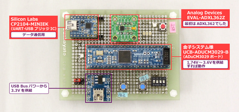
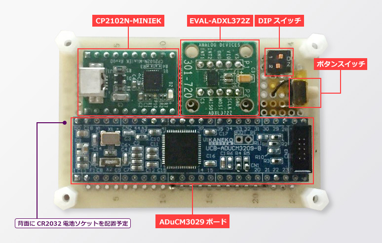
- ADI ADXL372 evaluation board EVAL-ADXL372Z
- Kaneko Systems ADuCM3029 board
- Silicon Labs CP2102N-MINIEK
* The configuration is not much different from Fig. 1. However, this is achieved with a 47x72mm universal board
- Power supply: 1 coin cell (CR2032)
- ADXL372 OPERATING MODES
* Make it possible to switch between these two with S / W
- Data output: COM port via USB bridge
- Development tools used: CCES 2.6.0 from ADI and emulator ICE-1000
From here, we will introduce the status of each development phase.
[Phase 1] First, verify using ADXL362
The board used in Phase 1 is the initial prototype board in Figure 1.
The ADuCM3029 development environment used CCES, which is the standard development environment for ADI's DSP/Processor products.
When using CCES, be sure to use Version 2.6.0 or later (latest 2.7.0: as of January 2018).
CCES is an Eclipse-based integrated development environment that uses GCC for the compiler. Of course, it also supports IAR and Keil instead of CCES, so you can use it in a familiar environment.
In addition, CCES has the familiar "CMSIS Pack Manager" installed in the Keil environment.
Phase 1 goal
In Phase 1, development proceeded with the following goals.
- Determine the state of the DIP switch and separate the routine that blinks the LED and the routine that operates the ADXL362.
- When the ADXL362 exceeds the threshold value (4g), the sampling data is stored in the built-in FIFO of the ADXL362 and an INT1 interrupt is generated.
- The ADuCM3029 waits after initial settings (GPIO, SPI, UART, interrupt, ADXL362).
- If there is an interrupt from ADXL362, perform FIFO read via SPI.
- The button switch is used as an interrupt source, and when this interrupt occurs, data is output to the PC via UART.
Developing an app for the ADuCM3029
I started developing the app immediately.
The ADuCM3029 evaluation board (UCM3029EZLITE) features the ADXL363. When I checked CMSIS Pack Manager, I found that a driver for ADXL363 and sample code were prepared. I decided to build on this basis.
Learn more about the ADuCM3029
Ultra-low power consumption is the biggest attraction Arm® Cortex®-M3 MCU ADuCM3029
First, when I checked the difference between ADXL362 and 363, it turned out that the register arrangement was completely different. Based on the data sheet, steadily create a register map for ADXL362. In consideration of changing to ADXL372 in the future, each instruction was ported to ADXL362 based on the source code of the driver for ADXL363.
Coding/Build work proceeded to the operation check without any particular problems.
Interrupt doesn't work...
Switching apps with the DIP switch works fine, and the L blinking works without any problems.
Now, it is finally time to check the operation of the ADXL362.
yeah? It doesn't move...
I thought it wouldn't go smoothly, but...
By stepping and displaying debug information in the Console Window, I was able to confirm that there was no problem with the R/W to the ADXL362 via SPI and that the register settings were correct. Using an oscilloscope, check that the interrupt signal from the ADXL362 is also output.
Further investigation revealed that there was a problem in the interrupt handling.
I was getting an error in the code I ported from the driver. This driver has a very deep hierarchy, and it is difficult to follow the code. . .
I know I'm missing some settings, but I don't know where the influence comes from, and only time passes. (Sweat) Other work is also busy, and at this time it's already July...
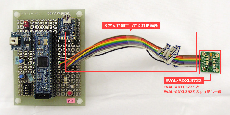
At that time, Mr. S modified the ADXL372 evaluation board to make it easier to give a shock.
Taking this opportunity, I decided to give up the operation check on the ADXL362 base and proceed to the ADXL372 base.
Not a defeat. I was able to confirm access with SPI, which was unconfirmed until now. regrettable. (tears)
However, this decision turned out to be good.
[Phase 2] Verification using production sensor ADXL372
Now, we have finally moved on to the phase of development using the ADXL372.
Learn more about the ADXL372
What is the "ADXL372" accelerometer that operates on a coin battery?
The board used in Phase 2 was an initial prototype board connected to the ADXL372 evaluation board that Mr. S had processed. The ADXL372 can detect large g (Max: 200g), and Mr. S's modification makes it easier to apply shocks than before.
Goal of Phase 2
The three goals for Phase 2 are:
- Operation check of ADXL372 (Operation check of 2 modes: Switch by DIP switch)
- Instant on mode
- Peak detection mode
- ADuCM3029 transitions to Hibernate mode after each initialization. Return to Active mode with a button switch as a trigger
- After recovery, perform FIFO read of ADXL372 and output data via UART (COM port). Transition to Hibernate mode again
Application development using drivers
In phase 2, we will check the basic operations that will be realized in the demo. Since I was having problems with interrupt handling in phase 1, the first thing I was worried about was, "How do I build the app?"
Inherit the driver-based app for ADXL363 used in Phase 1? Do you want to remake it with Scratch?
You also need to consider the time you have left.
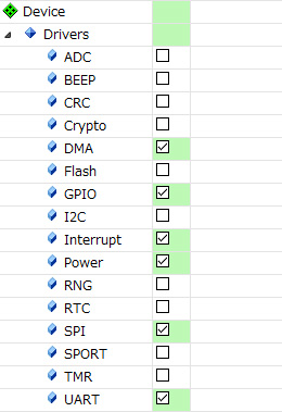
As a result, we decided to use the drivers prepared for each peripheral instead of the ADXL363 driver base used in Phase 1.
I used SPI/UART/Interrupt/Power/DMA/GPIO drivers.
Comparing the register maps of the ADXL362 and ADXL372 used in Phase 1, they are quite similar. Of course, there were some parts that had been expanded, and some changes were necessary, but this work was completed relatively easily and smoothly. (Phase 1 work helped!)
As for the coding itself, I referred to the sample code using each driver and proceeded with the work with the documentation of each driver in hand. There were no particular problems with this either.
Finally, it's time to test the machine.
This time, the interrupt moved easily
First, check from the interrupt operation that failed (tears) in phase 1.
In phase 1, we used the interrupt signal from the ADXL362, but this time we changed it so that the interrupt signal is generated by the button switch. The reason is to make the data output of UART arbitrary timing.
I set a breakpoint at the beginning of the interrupt routine, and when I pressed the button switch fearfully, I was able to easily check the operation.
that? What was the failure of Phase 1?
If you do it this way from the beginning...
No, you should learn a lot from your failures! Say to yourself and move on.
Verifying ADXL372 Operation – Instant On Mode
Now it's time to check the operation of the ADXL372.
First of all, I started checking the operation from the instant on mode. The settings for the ADXL372 are as follows.
- FIFO settings (Refer to Effective Use of the ADXL372 Internal FIFO)
- Stores X, Y and Z axis acceleration data
- Number of FIFOs: 120 stages (3 axes x 40 sets)
- Mode: Oldest save mode
- Power control settings
- Threshold level: Low (10g-15g)
- Filter Settling Time: 370ms
- Instant on mode
- Measurement control settings
- Auto Sleep Mode / Loop Mode (see datasheet)
- 4-pole low-pass filter bandwidth: 200Hz
- ODR: 400Hz
Instant-on mode test results
In this demonstration, Silicon Labs' CP2102N (UART-USB bridge IC) is installed for communication, so the result is output to the COM port (using Tera Term). Here is the output result.
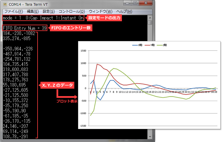
As far as the output result is concerned, you can see that it is working.
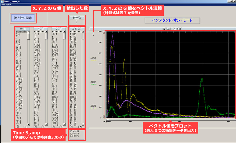
The scale factor of the ADXL372 is 100mg/LSB, so we know that we measured an acceleration of -108g on the Z axis. This data is the result of playing the ADXL372 board strongly once. After detecting the impact, you can see that it will gradually end.
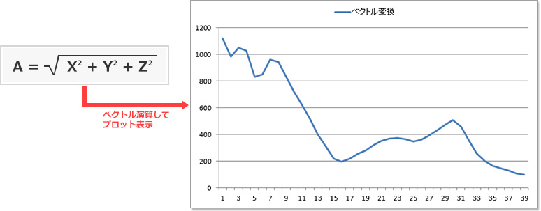
I also tried vector math. As far as the results (Fig. 4) are concerned, the data is "rough", so we thought that adjustments such as increasing the number of FIFOs and speeding up the ODR were necessary.
Verifying ADXL372 Operation – Peak Detect Mode
Furthermore, peak detection was set as follows and the operation was confirmed.
- FIFO settings: same as instant on mode
- Setting each threshold
- ACT Threshold (X, Y, Z): 4G
- ACT time: 6.6ms (Min value)
- INACT threshold (X, Y, Z): 2G
- INACT time: 130ms (26ms x 5)
- Power control settings
- Filter Settling Time: 370ms
- Full measurement mode
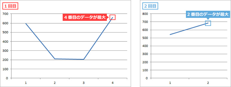
Peak detection mode test results
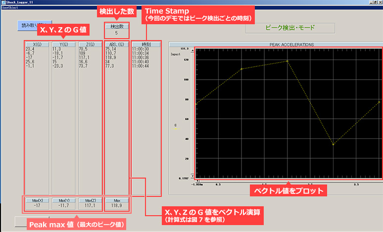
In the test, after playing the ADXL372 module four times, the data was output once. After playing it twice, I tried to output the data again. The result was printed as follows.
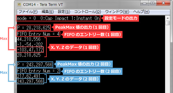
Peak Max contains the maximum value in the FIFO.
I tried vector math.
We have confirmed the basic operation of the instant on mode and peak detection mode.
Phase 2 went smoothly without any major problems. I was relieved that I could see the future a little, but I will need to make adjustments from now on. Moving on to Phase 3!
Effective use of the internal FIFO of the ADXL372
Here, we will introduce the FIFO built into the ADXL372.
Effective use of the FIFO allows the ADXL372 to operate autonomously. This has the effect of minimizing the involvement of the microcomputer and increasing the contribution to low power consumption at the system level.
Flexible settings are possible! 512-stage FIFO
512 levels of FIFO are prepared and can be assigned arbitrarily as follows.
- Up to 170 sample sets of triaxial data
- Up to 256 sample sets of biaxial data (user selectable)
- Up to 512 sample sets of single-axis data
- Up to 170 sets of collision event peaks (X, Y, Z)
Furthermore, the following modes are prepared as modes for saving data.
Oldest save mode
Accumulates data until the FIFO is full and holds it until the data is read out (this is the mode used in this demo).
stream mode
Always store new data in FIFO, delete the oldest data when new data arrives
Trigger mode
FIFO behaves like stream mode until an active detection event occurs, after which it stores pre- and post-event samples
In this way, it can be used flexibly according to the user application.
Considerations When Using the ADXL372 Internal FIFO
There is one point to note here, regarding the use of FIFO.
In the phase 2 instant on mode setting, the number of FIFO settings is set to "40Set". However, in Figure 6, the number of FIFO entries is "39", and the data actually output is also "39". This is done on purpose. This is because the data sheet has the following notes as points to note when reading the FIFO, and I processed it according to this.
"When reading multiple axes of data from the FIFO, at least one set of samples must remain on the FIFO after each read to prevent data from being overwritten or stored in the wrong order (hence , the number of samples in a triaxial data set must be at most 169.”
[Phase 3] Operation check and further improvement on production demo machine
Finally, it's time to test on the demo machine.
By this time, it was already August. Mr. S, who is working with me, assembled a demo machine based on the pin arrangement we specified, despite being very busy.
One month left to assemble the demo machine
Figure 6 has a button switch. However, it is not in the final block diagram of Figure 7.
Actually, at first, this button switch was used as one interrupt factor, but it was changed in the middle, and it is not wired anywhere in the completed demo machine. I would like to touch on this a little later.
I also added a DIP switch. There are two reasons.
- To determine the initial mode of operation of the ADXL372 during POR
- To determine the boot mode of the ADuCM3029
Boot mode has two modes: UART download mode and Flash boot mode.
When debugging, even if you write an application that behaves unexpectedly in Flash, if the environment allows UART boot, you can Erase/Write the Flash externally with a dedicated tool. I think it's better to prepare a mechanism to switch Boot mode.
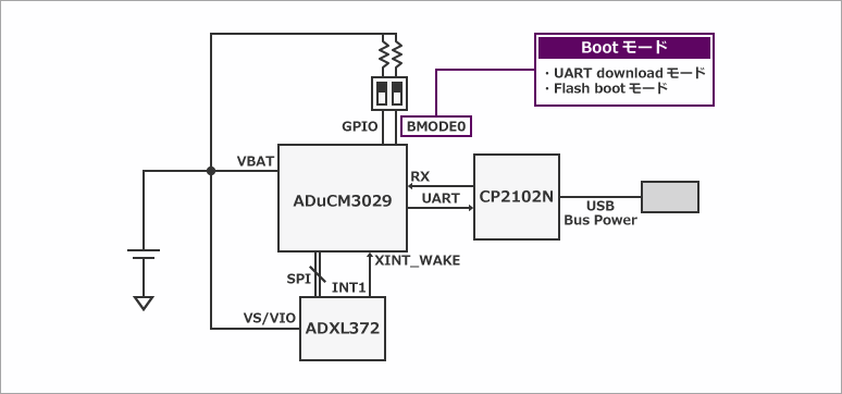
In Phase 3, instead of battery power, we used the function of Silicon Labs' USB bridge IC CP2102N to operate using USB Bus power. Since the CP2102N has a built-in regulator, it can generate 3.3V from Bus power (5V) and supply it externally, so I used it.
Chattering occurs when pressed or touched!
We started checking the operation based on the code created in Phase 2. I was able to confirm the basic operation, so I will proceed smoothly. However, I have come across a point of concern. It's a button switch.
This button switch plays an important role in determining the timing of the UART output. This will wake up the ADuCM3029 and start the UART output.
When I checked it, "chattering" occurred frequently when I pressed the button. For the time being, I tried to prevent chatter by using software such as Timer, but I couldn't prevent it.
At this point, I noticed something. A phenomenon occurs in which the signal chatters just by touching the button. (The chattering occurs even when the side of the button is touched.) Therefore, we asked them to take measures to prevent this by using additional resistors/capacitors and insulating tape, but we were unable to avoid it 100%.
Solved by stopping the button switch
So, I decided to stop using the button switch.
Then, what is the timing to wake up the ADuCM3029? The following are prepared as return factors from Hibernate mode.
- External interrupt
- UART RX interrupt
- RTC interrupt
- Power on Reset
Of these, we decided to use the UART RX interrupt (a Wake Up interrupt is generated when the UART RX line transitions), and eliminated the button switch.
4 improvements to further improve perfection
At this point, we temporarily released the test code we created and checked the operation in parallel with Mr. S. As a result, we identified four areas for improvement, and further aligned the phases for the finished product.
Improvement 1: Strengthen GND
In rare cases, the operation became unstable, so the problem was solved by strengthening the GND plane.
Improvement 2: Change to battery operation
This is what I expected from the beginning. Mr. S installed the battery holder.
Enhancement 3: Wake Up interrupt change for ADuCM3029
Changed to wake up by UART RX signal when returning from Hibernate mode.
Of course, the command to set Hibernate mode in the driver is also prepared, but I can't master it... In the end, I didn't use the driver for this part, wrote the C language myself, and confirmed the operation. (This is a point to be confirmed in the future.)
Improvement 4: Change board control itself to command interpreter via UART
Supports command interpreter for control from GUI. In addition, to make it easier to check the operation of the ADXL372, some register settings can be changed from the GUI.
Ported code proven in other microcomputers. I was able to confirm the operation of this as well. This eliminates the code modification / ReBuild / Download process that had been performed every time the ADXL372 register value was changed, making it possible to modify the ADXL372 register via UART (COM port). In addition, Mr. S created the GUI for this demo based on this command.
[Phase 4] Race Against Time! Final adjustments for completion
Finally, we enter the final phase.
The work was done in parallel with normal work, and at this time, it was already September, and it was a race against time. From here on, it will be the final adjustment that is conscious of the "how to present" to the seminar attendees.
Conscious of how to show the demo, final adjustment until the last minute
At this point, we discussed with the people concerned about how the demo should be presented, and made final adjustments.
Final Tweak 1: Increasing the number of FIFOs
The number of FIFO settings used in the current test is 40sets. Expand this to Max's 170 minute set.
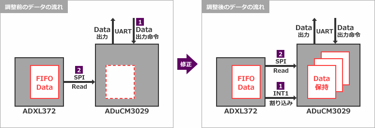
Final Tweak 2: Handling Impact Data in Instant On Mode
Instant-on mode performs automatic measurement until the FIFO is full when an impact exceeding the threshold is detected. The FIFO holds data until it is read or initialized, and is set so that new data cannot be acquired.
Therefore, only one impact data could be measured with one data output. This has been modified so that up to 3 impact data can be measured.
To measure up to three pieces of data, the INT1 pin of the ADXL372 was used to generate an interrupt when the FIFO was full. This interrupt wakes up the ADuCM3029 from Hibernate mode, reads shock data via SPI, and stores it in internal RAM. After that, I changed ADXL372 ⇒ instant on mode, ADuCM3029 ⇒ Hibernate mode, and waited in ultra-low power consumption mode.
Final Tweak 3: Adding Time Stamp Data
In order to get an image closer to the actual application, I decided to add a Time Stamp when the impact event occurred.
The ADuCM3029 has two built-in Real Time Clocks (RTCs), and the specified RTC continues to operate (continue counting) even after transitioning to Hibernate mode.
This time, we used the internal oscillator (LFOSC) as the clock source for the RTC and counted the time at 1Hz. Fixed so that the RTC count value is held in internal RAM in each mode and timing and output together when impact data is output.
<Instant On Mode>
- INT1 interrupt is generated when FIFO is full (timing of final adjustment 2)
- Hold RTC count value in internal RAM before FIFO Read (maximum 3)
<Peak detection mode>
- Generates INT1 interrupt when transitioning from ACT to INACT (when INACT is detected)
- Retains RTC count value in internal RAM (maximum 170)
This RTC is set in the initialization routine and starts the RTC count. In this demo, the RTC count value was passed to the host (PC), and the time at which the impact event occurred was calculated from this count value.
Full picture of shock detection demo
There were many twists and turns, but I managed to build the demo to the extent that it could be unveiled. (Although there are still some issues...) Here, I will introduce the state of the demo.
Demonstration with the image of luggage
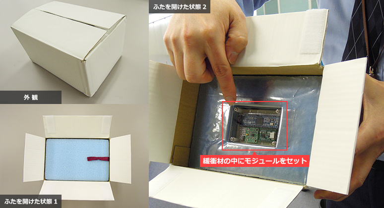
In this shock detection demo, Mr. S handcrafted a "special box" based on the image of a package. Put the module in this and give a shock to the whole box.
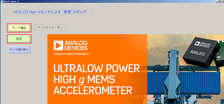
First, set the mode of the demo machine with the GUI
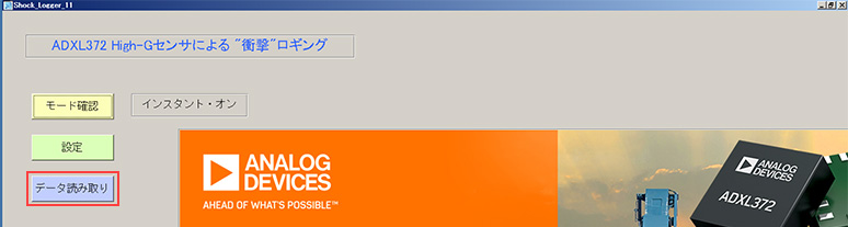
First, connect the host PC and the module via USB and set the mode. Confirm that the module is connected to the port, and start up the GUI.
Click the "Mode check" button to display the set mode. In addition, we are also checking the connection.
Demo in instant-on mode
First, try it in instant-on mode.
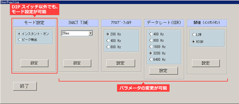
Install the demo unit in the packing box with the following settings.
Now let's give it a shock.
I tried dropping it from a height of about 1m. Repeat this 3 times.
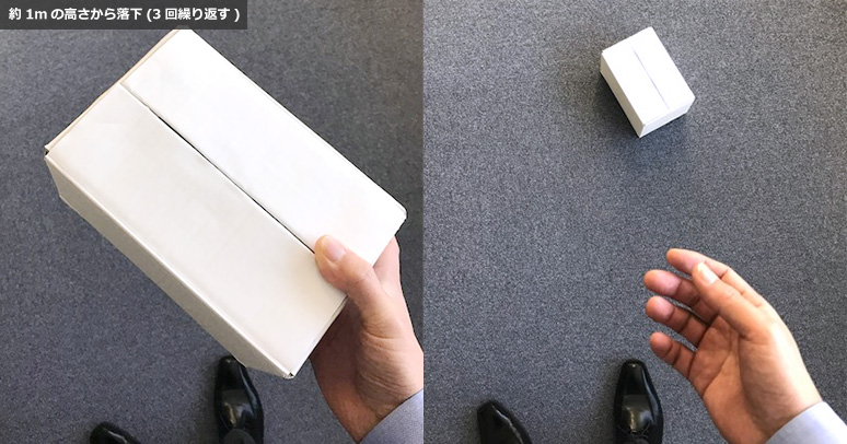
Take out the module from the packing box, connect to the GUI again, and click the "Read Data" button.
By displaying the data reading screen and clicking the "Start reading" button, we were able to obtain the data shown in Fig. 18.
Demo in peak detection mode
Next, I set it to peak detection mode and tested it in the same way.
This time it was dropped five times from random heights. The result is as follows.
Analog technology seminar was a great success on the day
We have introduced the process of creating a shock detection demo using ADI's ADXL372 + ADuCM3029. What do you think?
We successfully demonstrated it at the 2017 Analog Technology Seminar (hosted by ADI), so some of the visitors may have thought, "Oh, I've seen that before..." (Incidentally, we also exhibited it at Macnica booth at the ET2017 exhibition.)
On the day, all our hard work was worth it, as many customers showed interest!
Initially, we had planned to have customers throw the packaging boxes and print out the data, but unfortunately, due to the fact that many customers expressed interest in participating (space and time issues), we were unable to allow them to actually experience the demo. We would like to take this opportunity to apologize for this.
If you would like more information about the demo machine we created, the acceleration sensor and microcontroller used, other application examples, etc., please feel free to contact us.
Click here for recommended articles/materials
[Accelerometer ADXL372] Detects shock and vibration during transportation
What is the "ADXL372" accelerometer that operates on a coin battery?
Ultra-low power consumption is the biggest attraction Arm® Cortex®-M3 MCU ADuCM3029
Click here to purchase products
ADXL372BCCZ-RL7
EVAL-ADXL372Z (development tool)
ADUCM3029BCBZ-R7
ADUCM3029BCPZ-R7
ADZS-UCM3029EZLITE (development tool)
Click here for manufacturer site/other related links
ADXL372 Evaluation Board EVAL-ADXL372Z
ADXL372 Datasheet Rev.0 (PDF)
ADuCM3029 board
ADuCM3029 Data Sheet Rev.0 (PDF)
UCB-ADUCM3029-B User's Manual/Schematic (PDF)
ADuCM302x Hardware Reference Manual Rev1.0 (PDF)
Silicon Labs CP2102N-MINIEK