- Semiconductor BusinessHOME
- Products and Services of Macnica,Inc.
-
technical information

-
Events and Seminars
- Handling Manufacturer
- Support
- Inquiry
- Click here to purchase products
- Semiconductor business e-mail magazine registration
![]()
![]() Narrow down by specifying conditions
Narrow down by specifying conditions
現在2189件がヒットしています。check

This is a continuation of "Running DDR3 on Altera® FPGA! (Practical Edition) [1/2]".
3. Running a functional simulation
Next, let's run a functional simulation. The files required to run a simulation (such as a simulation project, test bench, traffic generator, and memory model) are automatically generated when you generate the controller, so you can run the simulation without any hassle.
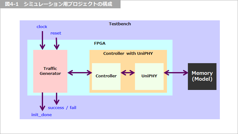
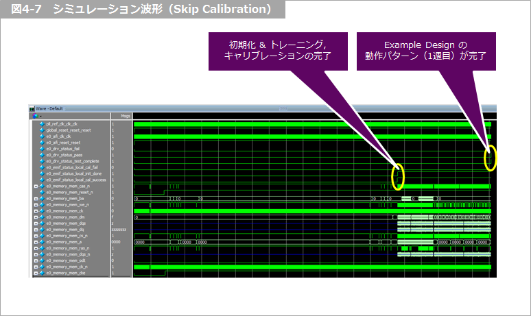
To briefly explain how the simulation works, the traffic generator receives a clock and sends addresses, commands, and data to the memory controller, which then writes them to the memory via UniPHY. The data read from the memory is then compared with the data written. If they match, Success = High; if they don't match, Fail = High.
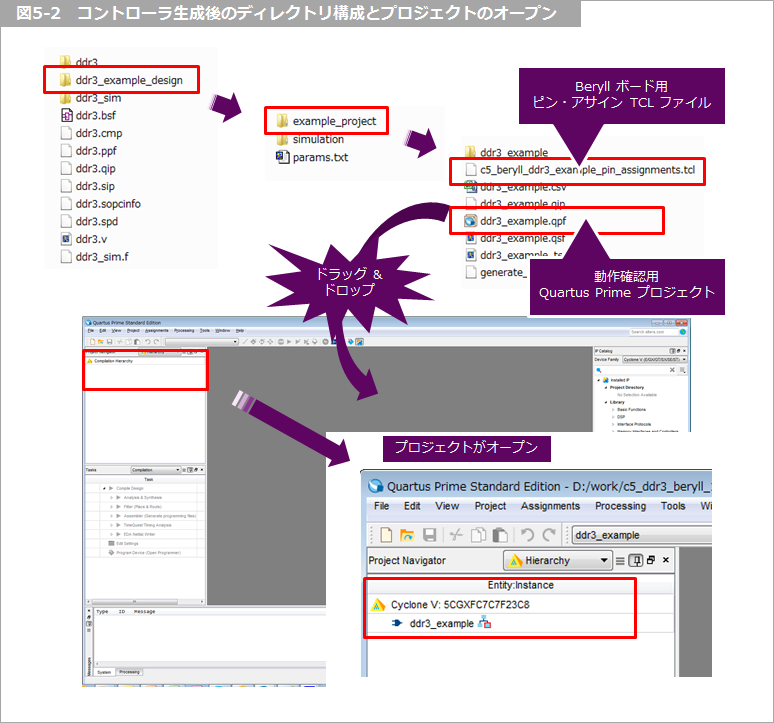
First, let's take a look at the directories and files after generating the controller!
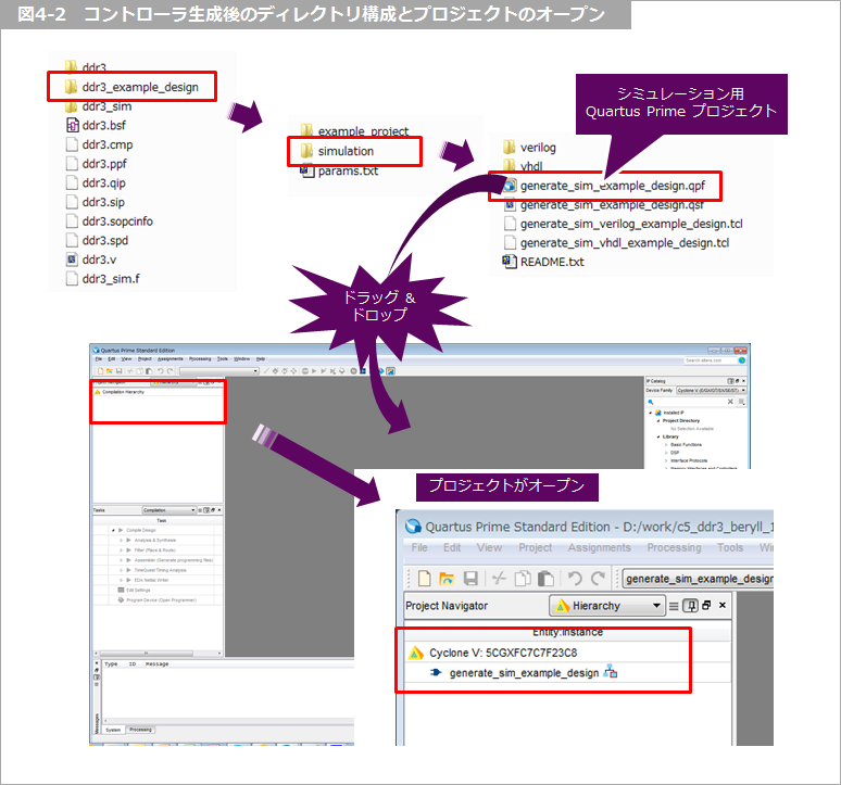
As shown in the image above, a Quartus® Prime project for simulation has been generated, so open it by selecting the simulation project (QPF file) from the File menu in Quartus® Prime and selecting Open Project. (You can also drag and drop the QPF file from Windows* Explorer into Quartus® Prime.)
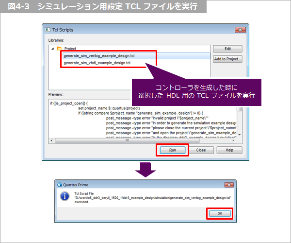
Once the project is open, select Quartus® Prime Tools ⇒ Tcl Scripts, select the simulation setup TCL file, and click Run to execute it. Be sure to select the HDL (Verilog or VHDL) you selected when generating the controller. This will also take a few minutes to complete. Once the TCL file has finished executing, click Close.
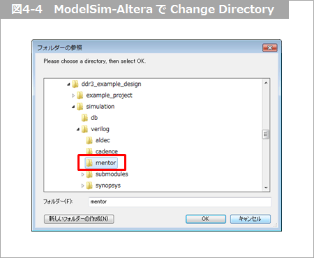
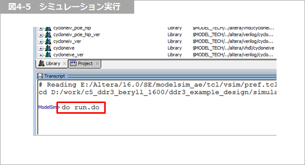
Next, start ModelSim® - Altera® FPGA Edition. After starting it, select File menu ⇒ Change Directory in ModelSim® - Altera® FPGA Edition and select the directory where the Example Design is stored ⇒ simulation ⇒ verilog or vhdl ⇒ mentor.
The DO file for running the simulation will be generated in the directory you moved to. Type "do run.do" in the Transcript window of ModelSim® - Altera® FPGA Edition and press Enter to run the simulation.
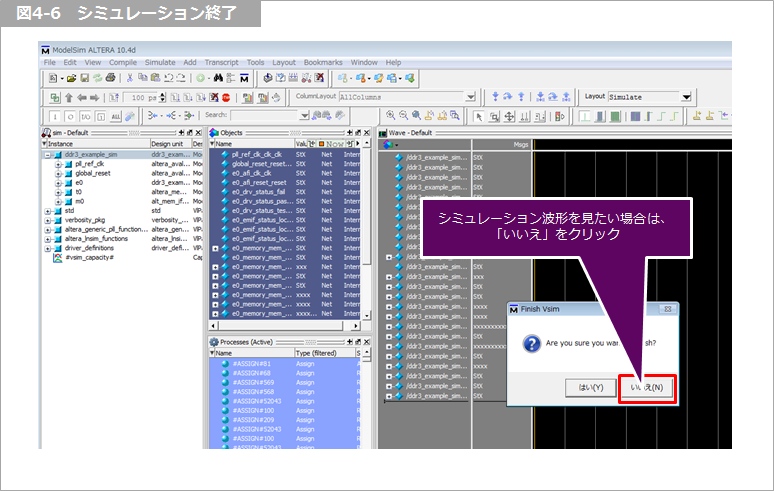
The simulation will take a few minutes to complete and will stop automatically once it is finished.
If the simulation is complete and you want to check the waveforms, click No. (Note that clicking Yes will close ModelSim® - Altera® FPGA Edition.)
4. Compiling the Example Design
Now let's compile the design for the Cyclone® V device on the Beryll board. Various settings, constraints, and pin assignments are required to compile.
If you have already purchased a Beryll board, you can download the circuit diagram and user guide from the dedicated Mpression page. While you can easily assign pins using these, we have prepared a TCL file for those viewing this page that allows you to easily assign pins for the DDR3 Example Design. After downloading this TCL file, save it in the Example Design project directory. You can also download the Beryll board circuit diagram specially from this page.
c5_beryll_ddr3_example_pin_assignments__1.tcl
Pin assignment TCL file for DDR3 SDRAM interface example design for Beryll board
Beryll Board Schematic (Rev.A)
Next, open the example design project for operation confirmation. In Quartus® Prime, select File menu ⇒ Open Project, select the project for operation confirmation (QPF file), and open the project. (You can also drag and drop the QPF file from Windows* Explorer into Quartus® Prime.)
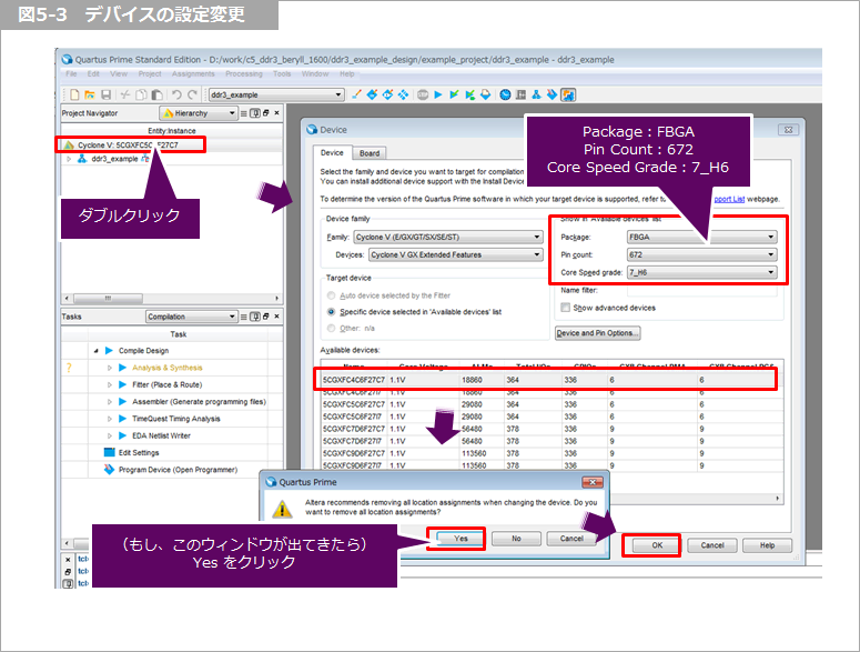
Once the project is open, change the device. The Beryll board is equipped with a Cyclone® V device with part number 5CGXFC4C6F27C7N, so set that part number. The last N in the part number indicates that it is lead-free. This N is not displayed in Quartus® Prime, so select 5CGXFC4C6F27C7.
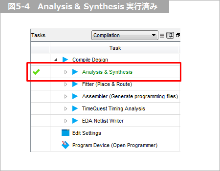
After opening the project for operation check, select Processing menu ⇒ Start ⇒ Start Analysis & Synthesis to execute logic synthesis. (Analysis & Synthesis in the Tasks window changes to a green check mark when logic synthesis completes successfully.
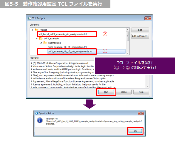
Select Tools menu ⇒ Tcl Scripts, select the TCL file in ①, and click Run. This is the TCL file that can be used to set the I/O Standard and other constraints for the DDR3 interface-related pins generated at the same time as the controller is generated.
Next, run the TCL file in ②. This is the pin assignment TCL file for the Beryll board mentioned earlier, and can be downloaded from within this article. If you did not save it in the project directory for the Example Design, it may not be displayed as shown here, so if you do not see it, please double-check the save location.
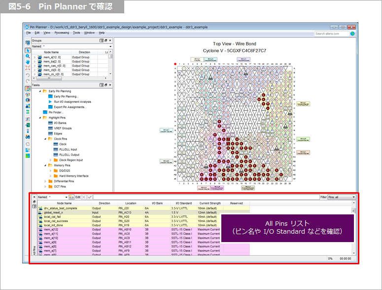
Launch the Pin Planner in the Quartus® Prime Assignments menu ⇒ Pin Planner to see if pin assignments and pin constraints have been made.
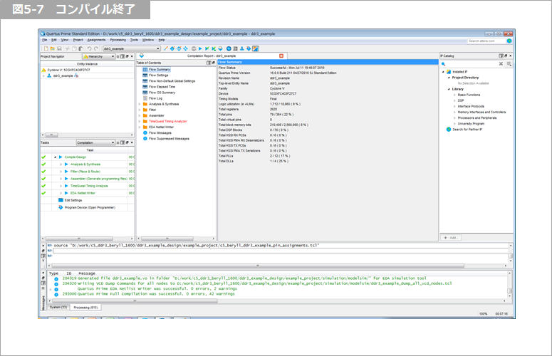
Once you've made it this far, let's compile. Select Quartus® Prime Processing menu ⇒ Start Compilation.
Did the compilation finish normally?
<Supplementary Note 1>
The timing analysis results (TimeQuest Timing Analyzer in the compilation report) are in red. This is because timing constraints have not been applied to all pins. However, since the unconstrained pins are pins for reset, JTAG, and LED output, we will proceed as is.
If you are experiencing timing violations in Setup or Hold, try changing the compilation settings. In Quartus® Prime, go to the Assignments menu, click Settings, click Compiler Settings, and then click Optimization mode. Set it to Performance. This setting prioritizes performance, so it tends to improve timing, but it can consume more resources.
<Supplementary Note 2>
If you want to change the memory controller settings, open ddr3.v, change the settings, and regenerate it. At this time, the pin information will be lost, so we recommend exporting the pin information before making changes.
[FAQ] Is there a way to export pin information from an existing project and import it into another project?
5. Operation check using Beryll board
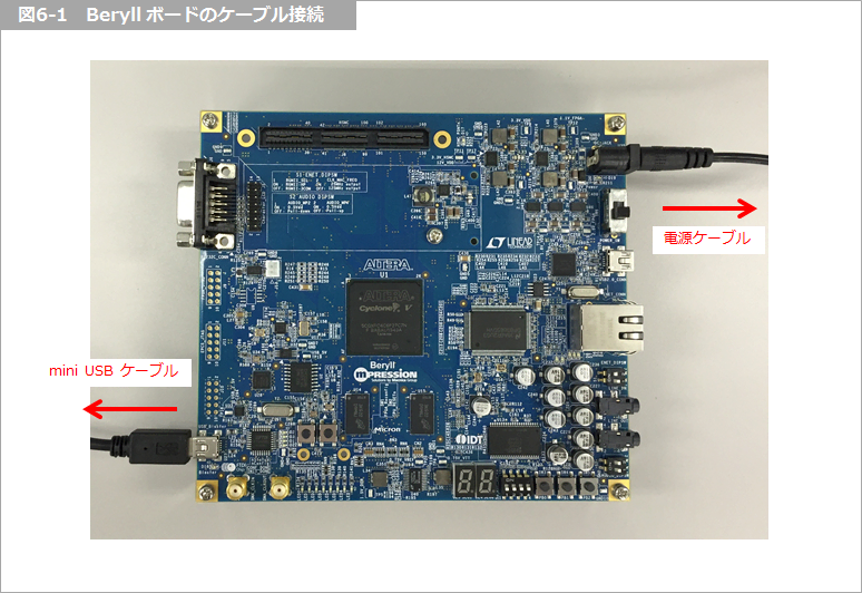
Once compilation is complete, write the SOF file generated by compilation to the Cyclone® V device. Connect the Beryll board to your PC with a USB cable (Beryll side: USB Mini-B) and turn on the power.
<Additional Information>
Altera® FPGAs have a JTAG port, through which data is written via an Altera® FPGA download cable.
Normally, an Altera® FPGA download cable (such as USB-Blaster™ or USB-Blaster™ II) is used, but the Beryll board has Blaster functionality implemented on the board, so there is no need to prepare a separate download cable; data can be written using just a USB cable.
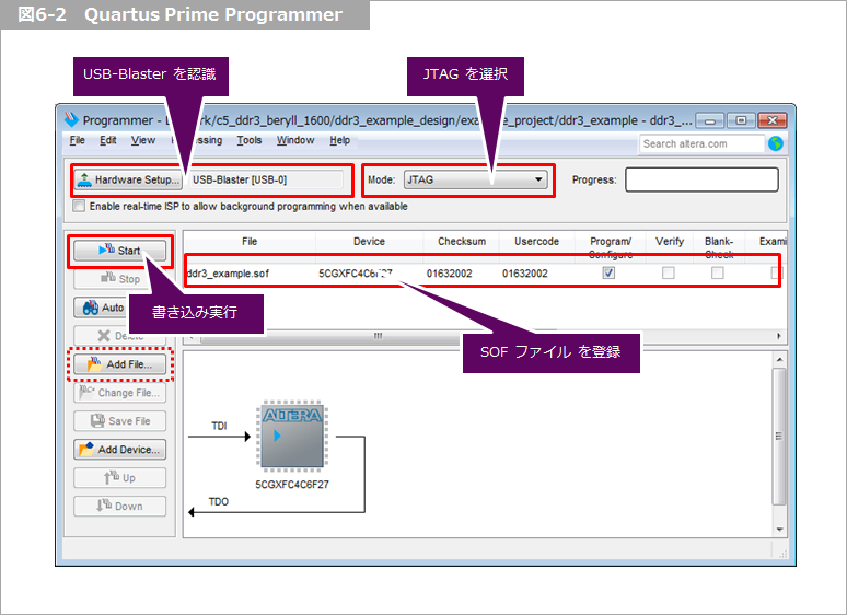
Then select Tools menu ⇒ Programmer in Quartus® Prime to launch the Quartus® Prime Programmer.
If the Programmer starts and the SOF file for writing is automatically registered, confirm that Hardware Setup and Mode are selected, then click Start to execute writing.
If the Programmer starts fresh, set the download cable, mode and burning file as follows, then click Start to execute burning.
- Hardware Setup: Select USB-Blaster™ (cannot be selected unless the USB-Blaster™ driver is installed)
- Mode: Select JTAG
- Add File: Select the SOF file generated during compilation (file name: <controller name>_example.sof)
After writing the SOF file, the Example Design is actually running. Under normal operation, LED2 and LED5 should be illuminated.
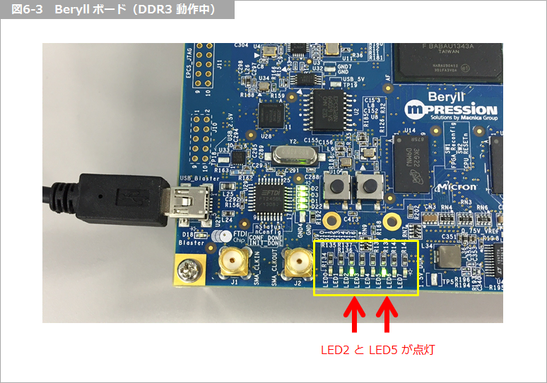
The pins are assigned in the TCL file, and the LEDs are assigned as shown in the table below. When the pin is at a low level, the LED lights up.
If you only look at this LED, you might not be able to tell if it is actually working. In that case, it might be interesting to incorporate logic that makes the LED blink while it is working.
You can also use the SignalTap® II logic analyzer to monitor internal FPGA signals, which I will cover on another occasion.
Table 6-1 Example Design pin description (partial)
| pin name | LED | explanation |
| local_Init_done | LED0 | Asserts high when memory initialization, training, and calibration are complete. |
| local_cal_success | LED1 | Asserted high upon successful completion of memory initialization, training, and calibration, indicating the controller is ready to use the memory interface. |
| local_cal_fail | LED2 | If memory initialization, training, or calibration fails, this signal is asserted high and local_init_done is not asserted. |
| drv_status_test_complete | LED3 | When the example design completes the first cycle of the memory write/read operation check pattern, this signal is asserted high. The simulation stops after one cycle, but the example design for operation check repeats the operation check pattern. |
| drv_status_pass | LED4 | When the example design successfully completes the first cycle of the memory write/read operation check pattern, this signal is asserted high. |
| drv_status_fail | LED5 | Asserts high if the example design fails to check the write/read operation pattern to memory. |
6. Summary
So far, I have explained along the agenda below, but did you get the image?
- Checking DDR3 SDRAM Support in Cyclone® V Devices
- Generating a DDR3 SDRAM Controller with UniPHY
- Running a functional simulation
- Compiling the Example Design
- Operation check using Beryll board
This article uses a Beryll board with a Cyclone® V device as an example, but the basic flow is the same for Stratix® series and Arria® series devices that support UniPHY-based DDR3 SDRAM controllers.
Please try to put this procedure into practice.
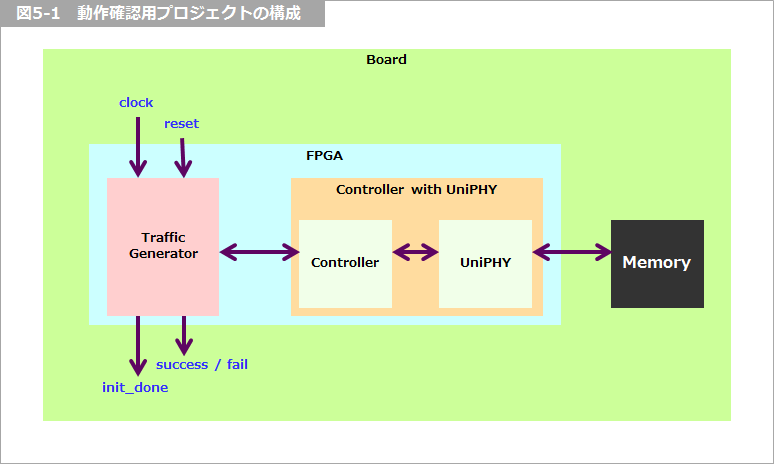
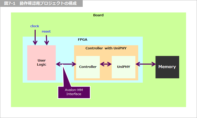
When actually incorporating this into your design, the Traffic Generator part of the Example Design will be replaced with your own logic, as shown in the figure below. The user logic and the controller will be connected via an Avalon-Memory Mapped (Avalon-MM) interface.
Click here for recommended articles/materials
EMIF Design & Debug Guidelines for FPGAs
Implementing an external memory controller in an Altera® FPGA!
Altera® FPGA Development Flow / Top Page
Click here for recommended FAQ
Manufacturer site/Other related links
External Memory Interface (Altera® site)
Avalon Interface Specification (Altera® website)