- 半導体事業HOME
- マクニカの製品・サービス
-
技術情報

-
イベント・セミナー
- 取扱メーカー
- サポート
- お問い合わせ
- 製品購入はこちら
- 半導体事業のメルマガ登録
![]()
![]() 条件を指定して絞り込む
条件を指定して絞り込む
現在2181件がヒットしています。check


こんにちは。
マクニカで Altera® FPGA の技術サポートをしている アルテラ ハナコ です。
今回の "Altera® FPGA で L チカ" は
Nios® V プロセッサー の登場です!
[関連情報] Nios® V プロセッサー (Altera) / Nios® V まとめページ (マクニカ)
基板上のプッシュボタンを押したときだけ LED が点灯し、プッシュボタンを離すと消灯する、
この動作を Nios® V ソフトコア・プロセッサー (以下 Nios® V) に制御させます。

※ HDL 言語の論理回路だけで L チカさせる方法は、こちら のコンテンツをご覧ください。
用意するもの
今回の開発環境は、これらを使用します。
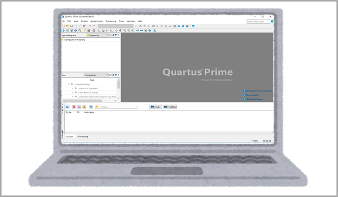
Quartus® Prime Standard Edition
または Lite Edition (無償)
&
Risc Free IDE for Altera
Questa* - Altera® FPGA Edition
または
Questa - Altera® FPGA Starter Edition (無償)

Nios® V の開発フロー

「プッシュボタンを押下したら LED が点灯し、プッシュボタンを離すと LED が消灯する」
この制御を Nios® V にさせるには、作業が大きく2つあります。
✔ FPGA に Nios® V を組み込む …… ハードウェア開発
✔ Nios® V に実行させるプログラム (C 言語) を作る …… ソフトウェア開発
今回の L チカ制御は HDL 言語だと簡単に書けてしまえますが
今回は 組み込み開発の作業フローを習得するために、簡単なデザインで Nios® V を使用してみましょう。
(これが Nios® V を採用した システム開発への第一歩です!)
Nios® V ライセンスファイルを取得する
Altera® FPGA の開発において Nios® V プロセッサー IP を利用するには、ライセンス費用は無償ですが、専用のライセンスファイルを取得する必要があります。
下記コンテンツを参考に、ライセンスファイルを取得してください。
<Notes> Nios® V には Nios® V/c、Nios® V/m、Nios® V/g があります。それぞれのライセンスが必要な場合は 個別に取得してください。
作業ステップ
今回のサンプルでは、以下の作業をおこないます。
1. Platform Designer で Nios® V と周辺回路を設計する
4. 制約を設定する
5. コンパイルをする
6. タイミングを検証する
(※ 以降は、Part 2: ソフトウェア開発 をご覧ください)
7. BSP プロジェクトを生成する
8. アプリケーション・プロジェクトを生成する
9. RiscFree IDE にインポートする
10. アプリケーションをビルド / デバッグする
11. Nios® V の Boot プログラムを FPGA のオンチップ・メモリーに組み込む
<Notes> Quartus® Prime の細かな操作は、Altera® FPGA の開発フロー をご覧ください。
1. Platform Designer で Nios® V と周辺回路を設計する
1-1. Quartus® Prime プロジェクトを作成
Quartus® Prime の下記メニューを選択し、プロジェクトを作成します。
File メニュー ➤ New Project Wizard
このサンプルでは、プロジェクト名と最上位エンティティー名を niosv_led_c10lp に設定します。
ターゲットデバイスは、Cyclone® 10 LP 評価キットに搭載されている 10CL025YU256I7G を選択します。

1-2. Nios® V システムを作成
Quartus® Prime の下記メニューから Platform Designer を起動し、Nios® V プロセッサーと周辺回路を作ります。
Tools メニュー ➤ Platform Designer
このサンプルで作成する Nios® V システム構成は、下図のとおりです。
今回のサンプルでは、 Nios® V の Boot メモリーおよび実行メモリーは、On-Chip RAM とします。

1-2-1. Nios® V Processor を追加
Platform Designer の左上に位置する IP Catalog から Nios V/m Microcontroller を追加します。

下記のオプションを適用します。
・ Enable Debug = On
・ Enable Reset from Debug Module = On
・ それ以外のオプション = デフォルト
[Finish] ボタンを押下します。
Messages タブ内にエラーが表示されますが、ここではこのまま進みます。
1-2-2. On-Chip Memory を追加
Nios® V と同様に、IP Catalog から On-Chip Memory (RAM or ROM) を追加し、下記のオプションを適用します。
・ Type: RAM (Writable)
・ Total memory size: 40960 bytes
・ Initialize memory content = On
・ それ以外のオプション = デフォルト
[Finish] ボタンを押下します。

1-2-3. PIO を追加
IP Catalog から PIO (Parallel I/O) を追加し、バス幅と入出力属性を指定します。
下図を参考に、プッシュボタン用 PIO と LED 用 PIO を作成し、それぞれ [Finish] ボタンを押下します。

1-2-4. JTAG UART を追加
printf デバッグを行うため、パソコンと JTAG インターフェース(USB-Blaster™ II 経由)で UART 通信する JTAG UART を作ります。
パラメーターはデフォルト設定のまま [Finish] ボタンを押下します。

1-2-5. 各コンポーネントの名前を変更
System Contents タブの Name 欄を右クリック選択し、[Rename] を選択します。

サンプルデザインでは、下表のとおりにします。
| 変更前の名称 | 変更後の名称 |
| intel_niosv_m_0 | niosv_cpu |
| onchip_memory2_0 | onchip_memory |
| pio_0 | pb_pio |
| pio_1 | led_pio |
| jtag_uart_0 | jtag_uart |
1-2-6. 各コンポーネントを接続
Connections 欄の白丸 (〇) をクリックし、黒丸 (●) に変更すると、各コンポーネントが接続されます。
サンプルプロジェクトでは、下図のように接続します。

1-2-7. 割り込みポートを接続
JTAG_UART から Nios® V への割り込みを接続するため、IRQ 列にある jtag_uart の Interrupt Sender の白丸 (〇) をクリックし、上図のように接続します。
値は優先順位を示しますが、今回は割り込みが 1本 なので 0 のままにします。
1-2-8. Nios® V の Reset Vector を設定
niosv_cpu の Name 部分をダブルクリックし、再度パラメーターの画面を表示します。
サンプルプロジェクトでは、Nios® V の Boot メモリーと実行メモリーを On-Chip RAM(onchip_memory)にするため、以下および下図のように設定します。
・ Reset Agent: onchip_memory.s1
・ Reset Offset: 0x00000000

1-2-9. PIO を Nios® V システムの外部に Export
pb_pio および led_pio の external_connection の Export 欄をそれぞれにダブルクリックし、ポートを作成します。

1-2-10. ベースアドレスを設定
ベースアドレスが重複のないように設定します。
下記メニューを実行し、ベースアドレスを適切な値に自動設定します。
Platform Designer の System メニュー ➤ Assign Base Address
1-2-11. Nios® V システムを保存

この Platform Designe の設定内容を保存するため、File メニュー ➤ Save を選択し、ファイルに名前を付け Quartus Prime プロジェクトフォルダーへ qsys ファイルを保存します。
このサンプルでは、niosv_system.qsys として保存します。
1-2-12. Nios® V システムのモジュールを生成
Generate メニュー ➤ Generate HDL を選択し、表示された Generation 画面において Synthesis / Simulation / Output Directory を指定します。

|
[Synthesis] Create HDL design files for synthesis: |
Quartus® Prime のコンパイルで使用する論理合成用の HDL 言語を指定します。 |
|
[Simulation] Create simulation model: |
シミュレーション用モデルの HDL 言語を指定します。
(サンプルでは Verilog を選択します。) <Notes> Windows 版の特定のバージョンにおいて、シミュレーション用モデルを選択し Generate を実行すると、Error が発生します。 詳細は 弊社の技術サポートへお問い合わせください。 |
|
[Output Directory] Path: |
ファイルを生成するフォルダーを指定します。 (サンプルではデフォルトのままにします。) |
Platform Designer 画面の右下にある [Generate] ボタンをクリックし、各種ファイルを生成します。
ファイルの生成が完了し Generate Completed ウインドウを [Close] ボタンで閉じた後、Platform Designer の右下にある [Finish] ボタンをクリックし、
Platform Designerを閉じます。
2. FPGA のデザインを完成させる
2-1. Nios® V システムをユーザーデザインにインプリメント

最上位階層の HDL デザインに Platform Designer で作成したシステムモジュールを組み込みます。
ユーザーデザインへ組み込みやすいように、Platform Designer で作成した Nios® V システムが保存されているフォルダー内に インスタンス補助ファイル(*_inst.vhd / *_inst.v)があるります。これらの記述内容をコピー&ペーストし、さらにコードを編集して接続を完了させます。
例えば、このような感じです。
![]() VHDL トップデザイン サンプル記述
VHDL トップデザイン サンプル記述 ![]() Verilog HDL トップデザイン サンプル記述
Verilog HDL トップデザイン サンプル記述
このサンプルでは、ファイル名を niosv_led_c10lp.vhd / niosv_led_c10lp.v として保存します。
最上位階層の HDL デザインを File メニュー ➤ Save As… でファイル名を付け保存します。

2-2. デザインを登録
HDL デザインと Nios® V システムを Quartus® Prime のプロジェクトに登録します。
Project メニュー ➤ Add/Remove Files in Project
作成した最上位の HDL デザイン (niosv_led_c10lp.vhd または niosv_led_c10lp.v) と、Nios® V システムの .qip ファイル (niosv_system.qip) を登録します。
同様に、このあと NativeLink で RTL シミュレーションを実行するために、Nios® V システムの .sip ファイルも登録しておきましょう。

なお
.qip は、Platform Designer で作成したモジュール用フォルダー/synthesis 内に生成されています。
.sip は、Platform Designer で作成したモジュール用フォルダー/simulation 内に生成されています。
<関連 FAQ> .sip ファイルとはどのようなファイルですか?
2-3. エラボレーション実行
Processing メニュー ➤ Start ➤ Start Analysis & Elaboration を実行します。
3. RTL シミュレーションをする
このサンプルでは、Nios® V のソフトウェア動作を含む Quartus Prime プロジェクト全体を RTL シミュレーションするフローをご紹介します。
3-1. ソフトウエア・プロジェクトを作成

事前に Quartus® Prime プロジェクトフォルダー内に、ソフトウエア開発用のワークスペース (フォルダー) を手動で作成します。
このサンプルでは、software フォルダーを作成します。
さらに、software フォルダー内に、アプリケーション・プロジェクト用フォルダー (app) と BSP 用フォルダー (hal_bsp) をそれぞれ作成します。
3-1-1. BSP (Board Support Package) の生成
Windows の スタート ➤ Altera <version.build_number> <Standard or Lite> Edition フォルダーを開き、Nios V Command Shell (Quartus Prime <version>) をクリックして、Nios V command shell を起動します。
Nios V command shell に下記コマンドを入力し、Quartus® Prime のプロジェクトフォルダーをカレントディレクトリーに指定します。
cd C:\AlteraFPGA_prj\niosv_sample
Nios V command shell に下記コマンドを入力し、BSP Editor を起動します。
niosv-bsp-editor
BSP Editor の File メニュー ➤ New BSP… を選択後、SOPC Infomation File Name 欄横のボタンを押下し、使用するハードウェア情報 (.sopcinfo ファイル) を BSP Editor に指定します。

BSP Editor のGUI が表示されます。今回のサンプルでは編集はおこなわず、GUI 右下の [Generate] をクリックします。
Information タブに Finished generating BSP files. が表示されたのを確認後 [Exit] します。

3-1-2. アプリケーション・プロジェクトの生成
あらかじめ作成しておいた Nios® V の Boot プログラム (C ソースファイル) を 先ほど作成した software/app フォルダーへ移動します。
このサンプルでは、ファイル名を presspb_led_niosv.c として保存します。
次に Nios V Command Shell へ 次のコマンドを入力します。
# アプリケーション・プロジェクト・ファイルの生成
niosv-app --bsp-dir=software/hal_bsp --app-dir=software/app --srcs=software/app/presspb_led_niosv.c --elf-name=presspb_led_niosv.elf
# アプリケーション・プロジェクトの構築
cmake -G "Unix Makefiles" -DCMAKE_BUILD_TYPE=Debug -B software/app/build/Debug -S software/app
make -C software/app/build/Debug
Nios® V の Boot プログラムが .elf として生成されます。
3-2. Hex ファイルの生成
今回のサンプルでは、Nios® V は FPGA の内蔵メモリー (Nios® V システムの On-Chip Memory) に格納したプログラムを Boot 時に実行します。
この Boot プログラムを RTL シミュレーションに反映させるため、次のコマンドを Nios V Command Shell へ入力し elf ファイルを hex ファイルに変換します。
elf2hex app/build/<user_applicatio>.elf -o <hex_output_file>.hex -w <On-Chip RAM のデータ幅> -b <On-Chip RAM の ベースアドレス> -e <On-Chip RAM の エンドアドレス>

例)
elf2hex software/app/build/Debug/presspb_led_niosv.elf -o software/app/niosv_system_onchip_memory.hex -w 32 -b 0x00010000 -e 0x00019FFF
<Notes>
Platform Designer で作成した On-chip Memory の初期値設定が
デフォルト (Initialize memory content = On) の場合は、
hex ファイル名は niosv_system_onchip_memory.hex にしてください。
もし、Enable non-default initialization file でデフォルト以外のファイルを
指定している場合は、elf2hex コマンドの -o を 目的のファイル名および
パス先で指定してください。
例) elf2hex software/app/build/Debug/presspb_led_niosv.elf -o ocram_init/niosv_boot.hex -w 32 -b 0x00010000 -e 0x00019FFF

次に、先ほど生成した niosv_system_onchip_memory.hex ファイルを、下記シミュレーション・モデルの保存フォルダーへコピーします。
<Quartus Prime プロジェクト>/<Platform Designer フォルダー>/simulation/submodules
今回のサンプルでは、以下のフォルダーへコピーします。
C:\AlteraFPGA_prj\niosv_sample\niosv_system\simulation\submodules

3-3. NativeLink シミュレーションの設定
Quartus® Prime 上で NativeLink を実行するための環境を構築します。(こちらのコンテンツ の "環境を設定する" を参考に、設定してください。)

次に Quartus® Prime の下記メニューで NativeLink シミュレーションの設定をおこないます。
Assignments メニュー ➤ Settings ➤ EDA Tool Settings ➤ Simulation
|
項目名 |
設定内容 |
| Tool name |
シミュレーションに使用する EDA ツール (今回のサンプルでは、Questa-Altera FPGA Edition を使用) |
| Format for output netlist |
Verilog HDL を選択 (VHDL 設計であっても、ここでは Verilog を指定してください。) |
| Output directory | デフォルト (simulation/<tool_name>) |
|
EDA Tool Settings 上部 (Simulation 内) |
|
| Compile test bench |
ユーザーのテストベンチを設定
作業フロー “3. NativeLink settings 内にて、テストベンチを登録します。” を参考にしてください。) |
|
EDA Tool Settings 下部 (Simulation 内) |
|


各ウインドウを OK で閉じます。
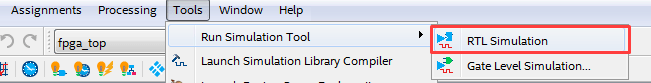
3-4. NativeLink で RTL シミュレーション実行
Tools メニュー ➤ Run Simulation Tool ➤ RTL Simulation をクリックします。
※ RTL Simulation 実行には、事前に Analysis & Elaboration または Analysis & Synthesis、あるいは Fitter のプロセスが実行されている必要があります。
ただし、Start Compilation (Processing メニュー) は実行しないでください。EDA Netlist Writer が自動的に実行されてしまい
正常な RTL Simulation 用のスクリプトが生成されない場合があります。
フルコンパイルを実行してしまった場合は、再度 Analysis & Elaboration または Analysis & Synthesis、あるいは Fitter を実行後に RTL Simulation をおこなってください。
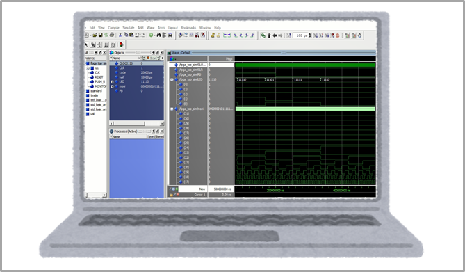
Wave ウインドウに波形が表示されます。

期待する動作になっていることを確認後、シミュレーションおよび Questa - Altera FPGA Edition を終了します。
<Notes>
今回のサンプルでは、プッシュボタンが押下されると Nios V が LED 用の PIO に 0xF を書き込み LED を点灯させ、プッシュボタンが離されていると Nios V が LED 用の PIO に 0x0 を書き込み
LED を消灯させる動作がシミュレーションにより確認できます。
また、presspb_led_niosv.c において指定した alt_printf 関数 "Hello from Nios V !!" が Transcript ウィンドウに表示されたことが確認できます。
Questa - Altera FPGA Edition の Simulate メニュー ➤ End Simulation、File メニュー ➤ Quit
その後、Quartus Prime の Assignments メニュー ➤ Settings ➤ EDA Tool Settings ➤ Simulation において、Tool name を <none> に戻します。
[参考]
NativeLink を活用せず Questa (Altera FPGA Edition を含む) でシミュレーションを実施する場合は
Platform Designer の生成フォルダー内にある シミュレーション用スクリプトファイル msim_setup.tcl をカスタマイズします。
/<Nios V システムのフォルダー>/simulation/mentor/msim_setup.tcl
msim_setup.tcl の編集や作業フローは、下記コンテンツを参考にしてください。
4. 制約を設定する
4-1. ピンアサインを設定
Quartus® Prime の Assignments メニュー ➤ Pin Planner を起動し、ユーザーデザインのピンを FPGA のピンへアサインします。
Cyclone® 10 LP 評価キットでは、以下のようにピンを設定してください。

4-2. タイミング制約を設定
Nios® V システム用の SDC は、qip ファイル生成時(操作 1-2-12. Nios® V システムのモジュールを生成)に自動生成され、qip ファイル登録と共に
Timing Analyzer (Assignments メニュー ➤ Settings) に適用されています。

その他、ユーザーデザインに対してタイミング制約を作成し、同様にプロジェクトに登録します。
今回のサンプルは 50MHz のクロックが供給され動作する仕様のため、クロック定義のコマンドを記述した SDC を作成し、プロジェクトに追加登録します。
このサンプルでは、ファイル名を niosv_led_c10lp.sdc として保存します。
<Notes>
このサンプルでも本来はユーザーデザイン用の SDC ファイルに I/O 制約が必要ですが、入力信号 (プッシュボタンを人が押す・離す) および 出力信号 (LED が点灯・消灯) が超低速なので、
ここでは I/O のタイミング制約を省略しています。

5. コンパイルをする
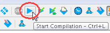
以下のメニューにより、コンパイルを実行します。
Processing メニュー ➤ Start Compilation
論理合成と配置配線が実行され、FPGA 内部に書き込むビットストリームデータ (.sof) も生成されます。
コンパイル終了後に、生成された コンパイル・レポートを検証 します。
6. タイミングを検証する

コンパイルレポート内の Timing Analyzer フォルダーを展開してタイミング検証をします。
各タイミングモデルがクロック周波数の制約条件を Pass したことが確認できます。
これで ハードウェアのデザイン作成は完了です。
仮に、Quartus Prime のコンパイルで生成された sof ファイルを FPGA に転送しても、内部の Nios® V が実行するためのプログラムが まだないため
評価ボード上のプッシュボタン [PB3] を押しても LED は消灯したままです。
では、続いて Nios® V のソフトウェア開発をしましょう。
![]() Altera® FPGA の Nios® V で はじめての L チカ! Part 2: ソフトウェア開発 (Quartus® Prime Standard Edition 編)
Altera® FPGA の Nios® V で はじめての L チカ! Part 2: ソフトウェア開発 (Quartus® Prime Standard Edition 編)
おすすめ記事/資料はこちら
FPGA のオンチップ・メモリーで Nios® II をブートさせてみよう
MAX® 10 の UFM で Nios® II をブートさせてみよう
おすすめオンラインセミナーおよびワークショップはこちら
Agilex™ 3 FPGA で Nios® V を動かしてみよう ("オンラインセミナーを受講したい" を参照ください)
Nios® V プロセッサー 入門 コース ("トレーニングを受講したい" を参照ください)